HFD2N90 Specs and Replacement
Type Designator: HFD2N90
Type of Transistor: MOSFET
Type of Control Channel: N-Channel
Absolute Maximum Ratings
Pd ⓘ - Maximum Power Dissipation: 70 W
|Vds|ⓘ - Maximum Drain-Source Voltage: 900 V
|Vgs|ⓘ - Maximum Gate-Source Voltage: 30 V
|Id| ⓘ - Maximum Drain Current: 2 A
Tj ⓘ - Maximum Junction Temperature: 150 °C
Electrical Characteristics
tr ⓘ - Rise Time: 55 nS
Cossⓘ - Output Capacitance: 70 pF
RDSonⓘ - Maximum Drain-Source On-State Resistance: 5.6 Ohm
Package: D-PAK
HFD2N90 substitution
- MOSFET ⓘ Cross-Reference Search
HFD2N90 datasheet
hfd2n90.pdf
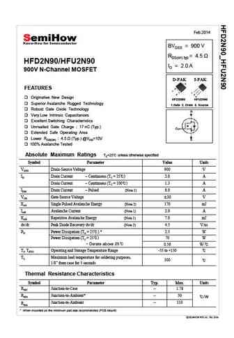
Feb 2014 BVDSS = 900 V RDS(on) typ HFD2N90/HFU2N90 ID = 2.0 A 900V N-Channel MOSFET D-PAK I-PAK 2 FEATURES 1 1 3 2 3 Originative New Design HFD2N90 HFU2N90 Superior Avalanche Rugged Technology 1.Gate 2. Drain 3. Source Robust Gate Oxide Technology Very Low Intrinsic Capacitances Excellent Switching Characteristics Unrivalled Gate Charge 17 nC (Typ.) ... See More ⇒
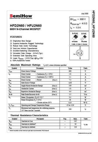
hfd2n60u hfu2n60u.pdf

June 2015 BVDSS = 600 V RDS(on) typ = 4 HFD2N60U / HFU2N60U ID = 1.8 A 600V N-Channel MOSFET D-PAK I-PAK FEATURES 2 1 Originative New Design 1 3 2 3 Superior Avalanche Rugged Technology HFD2N60U HFU2N60U Robust Gate Oxide Technology 1.Gate 2. Drain 3. Source Very Low Intrinsic Capacitances Excellent Switching Characteristics Unrivalled Gate Charge 5.5 nC (T... See More ⇒
hfd2n60u.pdf
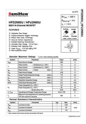
Jan 2014 BVDSS = 600 V RDS(on) typ = 4 HFD2N60U / HFU2N60U ID = 1.8 A 600V N-Channel MOSFET D-PAK I-PAK FEATURES 2 1 Originative New Design 1 3 2 3 Superior Avalanche Rugged Technology HFD2N60U HFU2N60U Robust Gate Oxide Technology 1.Gate 2. Drain 3. Source Very Low Intrinsic Capacitances Excellent Switching Characteristics Unrivalled Gate Charge 5.5 nC (Ty... See More ⇒
hfd2n65s.pdf
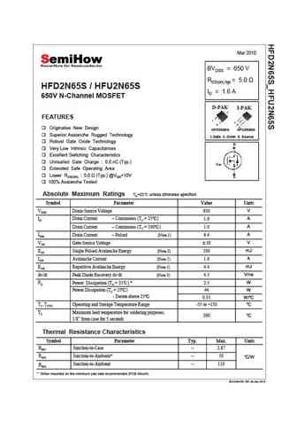
Mar 2010 BVDSS = 650 V RDS(on) typ = 5.0 HFD2N65S / HFU2N65S ID = 1.6 A 650V N-Channel MOSFET D-PAK I-PAK 2 2 FEATURES 1 1 3 2 3 Originative New Design HFD2N65S HFU2N65S Superior Avalanche Rugged Technology 1.Gate 2. Drain 3. Source Robust Gate Oxide Technology Very Low Intrinsic Capacitances Excellent Switching Characteristics Unrivalled Gate Charge 6.0 nC (Typ.... See More ⇒


Detailed specifications: HFD1N60S, HFD1N65S, HFD2N60, HFD2N60S, HFD2N60U, HFD2N65S, HFD2N65U, HFD2N70S, IRF2807, HFD3N80, HFD4N50, HFD5N40, HFD5N50S, HFD5N50U, HFD5N60S, HFD5N60U, HFD5N65S
Keywords - HFD2N90 MOSFET specs
HFD2N90 cross reference
HFD2N90 equivalent finder
HFD2N90 pdf lookup
HFD2N90 substitution
HFD2N90 replacement
Step-by-step guide to finding a MOSFET replacement. Cross-reference parts and ensure compatibility for your repair or project.
🌐 : EN ES РУ

LIST
Last Update
MOSFET: CM4407 | CM3407 | CM3400 | SVF11N65F | SVF11N65T | FKBB3105 | EHBA036R1 | CRTT067N10N | AP6NA3R2MT | AP65SA145DDT8
Popular searches
2sc627 | 2sc680 | 2sd234 | 2sc9014 | a970 transistor | 2sb560 | tip31c transistor equivalent | 2sc1815 datasheet