TSM2306CX Specs and Replacement
Type Designator: TSM2306CX
Type of Transistor: MOSFET
Type of Control Channel: N-Channel
Absolute Maximum Ratings
Pd ⓘ - Maximum Power Dissipation: 1.25 W
|Vds|ⓘ - Maximum Drain-Source Voltage: 30 V
|Vgs|ⓘ - Maximum Gate-Source Voltage: 20 V
|Id| ⓘ - Maximum Drain Current: 3.5 A
Tj ⓘ - Maximum Junction Temperature: 150 °C
Electrical Characteristics
tr ⓘ - Rise Time: 19 nS
Cossⓘ - Output Capacitance: 120 pF
RDSonⓘ - Maximum Drain-Source On-State Resistance: 0.057 Ohm
Package: SOT-23
TSM2306CX substitution
- MOSFET ⓘ Cross-Reference Search
TSM2306CX datasheet
tsm2306cx.pdf
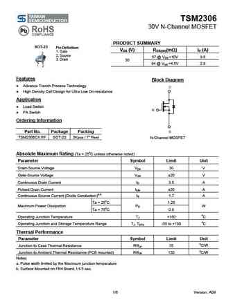
TSM2306 30V N-Channel MOSFET PRODUCT SUMMARY SOT-23 Pin Definition VDS (V) RDS(on)(m ) ID (A) 1. Gate 2. Source 57 @ VGS =10V 3.5 3. Drain 30 94 @ VGS =4.5V 2.8 Features Block Diagram Advance Trench Process Technology High Density Cell Design for Ultra Low On-resistance Application Load Switch PA Switch Ordering Information Part No. Pa... See More ⇒
tsm2301a.pdf
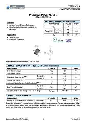
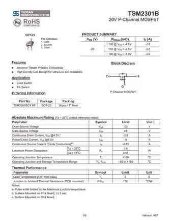
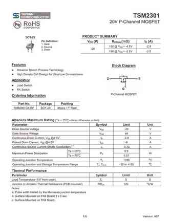
TSM2301A Taiwan Semiconductor P-Channel Power MOSFET -20V, -2.8A, 130m KEY PERFORMANCE PARAMETERS Features PARAMETER VALUE UNIT Advance Trench Process Technology VDS -20 V High Density Cell Design for Ultra Low On- resistance VGS = -4.5V 130 RDS(on) (max) m VGS = -2.5V 190 Application Qg 7.2 nC Telecom power Consumer Electronics SOT-23 ... See More ⇒
tsm2302 a07.pdf
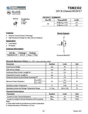
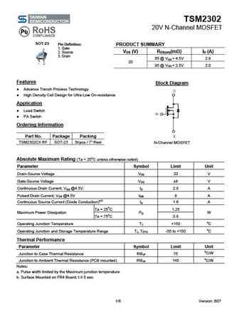
TSM2302 20V N-Channel MOSFET PRODUCT SUMMARY SOT-23 Pin Definition VDS (V) RDS(on)(m ) ID (A) 1. Gate 2. Source 65 @ VGS = 4.5V 2.8 3. Drain 20 95 @ VGS = 2.5V 2.0 Features Block Diagram Advance Trench Process Technology High Density Cell Design for Ultra Low On-resistance Application Load Switch PA Switch Ordering Information Part No.... See More ⇒
Detailed specifications: TSM20N50CZ, TSM210N06CZ, TSM2301ACX, TSM2301BCX, TSM2301CX, TSM2302CX, TSM2303CX, TSM2305CX, AON7403, TSM2307CX, TSM2308CX, TSM2310CX, TSM2311CX, TSM2312CX, TSM2313CX, TSM2314CX, TSM2318CX
Keywords - TSM2306CX MOSFET specs
TSM2306CX cross reference
TSM2306CX equivalent finder
TSM2306CX pdf lookup
TSM2306CX substitution
TSM2306CX replacement
Need a MOSFET replacement? Our guide shows you how to find a perfect substitute by comparing key parameters and specs
History: STP9NK50Z
🌐 : EN ES РУ

LIST
Last Update
MOSFET: AUP060N055 | AUP056N10 | AUP056N08BGL | AUP052N085 | AUP045N12 | AUP039N10 | AUP034N10 | AUP034N06 | AUP033N08BG | AUP026N085
Popular searches
tip31a datasheet | d882 datasheet | tip29 transistor | s9014 transistor datasheet | 2sa1491 | 2sc1313 datasheet | 2sc984 | 2sa872