TSM2314CX Specs and Replacement
Type Designator: TSM2314CX
Type of Transistor: MOSFET
Type of Control Channel: N-Channel
Absolute Maximum Ratings
Pd ⓘ - Maximum Power Dissipation: 1.25 W
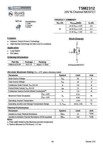
|Vds|ⓘ - Maximum Drain-Source Voltage: 20 V
|Vgs|ⓘ - Maximum Gate-Source Voltage: 12 V
|Id| ⓘ - Maximum Drain Current: 4.9 A
Tj ⓘ - Maximum Junction Temperature: 150 °C
Electrical Characteristics
tr ⓘ - Rise Time: 1.4 nS
Cossⓘ - Output Capacitance: 140 pF
RDSonⓘ - Maximum Drain-Source On-State Resistance: 0.033 Ohm
Package: SOT-23
TSM2314CX substitution
- MOSFET ⓘ Cross-Reference Search
TSM2314CX datasheet
tsm2314cx.pdf
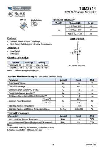
TSM2314 20V N-Channel MOSFET SOT-23 PRODUCT SUMMARY Pin Definition 1. Gate VDS (V) RDS(on)(m ) ID (A) 2. Source 3. Drain 33 @ VGS = 4.5V 4.9 40 @ VGS = 2.5V 4.4 20 100 @ VGS = 1.8V 2.9 Features Block Diagram Advance Trench Process Technology High Density Cell Design for Ultra Low On-resistance Application Load Switch PA Switch Orderin... See More ⇒
tsm2314cx.pdf

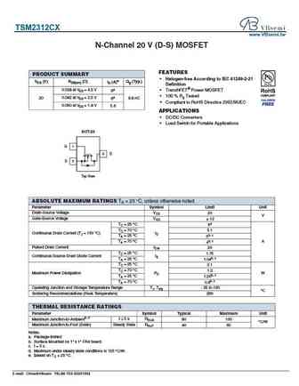
TSM2314CX www.VBsemi.tw N-Channel 20 V (D-S) MOSFET FEATURES PRODUCT SUMMARY Halogen-free According to IEC 61249-2-21 VDS (V) RDS(on) ( ) ID (A)e Qg (Typ.) Definition 0.028 at VGS = 4.5 V TrenchFET Power MOSFET 6a 100 % Rg Tested 20 0.042 at VGS = 2.5 V 6a 8.8 nC Compliant to RoHS Directive 2002/95/EC 0.050 at VGS = 1.8 V 5.6 APPLICATIONS DC/DC... See More ⇒
tsm2311cx.pdf
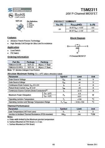
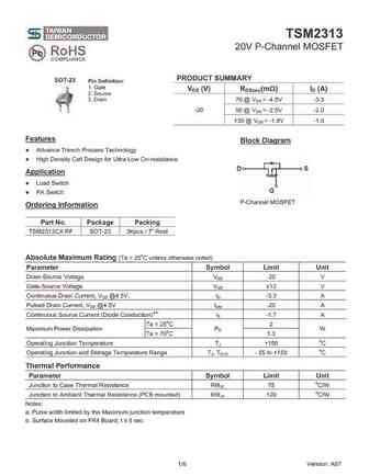
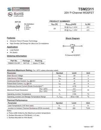
TSM2311 20V P-Channel MOSFET SOT-23 Pin Definition PRODUCT SUMMARY 1. Gate VDS (V) RDS(on)(m ) ID (A) 2. Source 3. Drain 55 @ VGS = -4.5V -4.0 -20 85 @ VGS = -2.5V -2.5 Features Block Diagram Advance Trench Process Technology High Density Cell Design for Ultra Low On-resistance Application Load Switch PA Switch P-Channel MOSFET Orderi... See More ⇒
Detailed specifications: TSM2305CX, TSM2306CX, TSM2307CX, TSM2308CX, TSM2310CX, TSM2311CX, TSM2312CX, TSM2313CX, 60N06, TSM2318CX, TSM2323CX, TSM2328CX, TSM23N50CN, TSM25N03CP, TSM2611EDCX6, TSM2N60CH, TSM2N60CP
Keywords - TSM2314CX MOSFET specs
TSM2314CX cross reference
TSM2314CX equivalent finder
TSM2314CX pdf lookup
TSM2314CX substitution
TSM2314CX replacement
Learn how to find the right MOSFET substitute. A guide to cross-reference, check specs and replace MOSFETs in your circuits.
History: TSM2307CX | STP9NK50Z | TSM2306CX
🌐 : EN ES РУ

LIST
Last Update
MOSFET: AUP060N055 | AUP056N10 | AUP056N08BGL | AUP052N085 | AUP045N12 | AUP039N10 | AUP034N10 | AUP034N06 | AUP033N08BG | AUP026N085
Popular searches
2sa872 | 2sc1222 | 2sc2581 | c1061 transistor | 2sc1451 | c3199 transistor | 2n2712 datasheet | 2sc2525