TSM2323CX Specs and Replacement
Type Designator: TSM2323CX
Type of Transistor: MOSFET
Type of Control Channel: P-Channel
Absolute Maximum Ratings
Pd ⓘ
- Maximum Power Dissipation: 1.25 W
|Vds|ⓘ - Maximum Drain-Source Voltage: 20 V
|Vgs|ⓘ - Maximum Gate-Source Voltage: 8 V
|Id| ⓘ - Maximum Drain Current: 4.7 A
Tj ⓘ - Maximum Junction Temperature: 150 °C
Electrical Characteristics
tr ⓘ - Rise Time: 43 nS
Cossⓘ -
Output Capacitance: 191 pF
RDSonⓘ - Maximum Drain-Source On-State Resistance: 0.039 Ohm
Package: SOT-23
- MOSFET ⓘ Cross-Reference Search
TSM2323CX datasheet
..1. Size:253K taiwansemi
tsm2323cx.pdf 

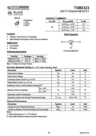
TSM2323 20V P-Channel MOSFET SOT-23 PRODUCT SUMMARY Pin Definition VDS (V) RDS(on)(m ) ID (A) 1. Gate 2. Source 39 @ VGS = -4.5V -4.7 3. Drain -20 52 @ VGS = -2.5V -4.1 68 @ VGS = -1.8V -2.0 Features Block Diagram Advance Trench Process Technology High Density Cell Design for Ultra Low On-resistance Application Load Switch PA Switch P-C... See More ⇒
7.1. Size:366K taiwansemi
tsm2323 a07.pdf 

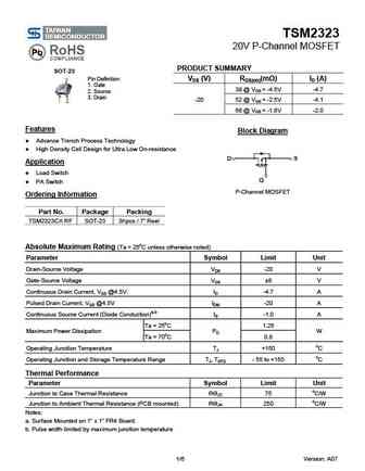
TSM2323 20V P-Channel MOSFET PRODUCT SUMMARY SOT-23 Pin Definition VDS (V) RDS(on)(m ) ID (A) 1. Gate 39 @ VGS = -4.5V -4.7 2. Source 3. Drain -20 52 @ VGS = -2.5V -4.1 68 @ VGS = -1.8V -2.0 Features Block Diagram Advance Trench Process Technology High Density Cell Design for Ultra Low On-resistance Application Load Switch PA Switch P-Chann... See More ⇒
8.1. Size:60K taiwansemi
tsm2328cx.pdf 

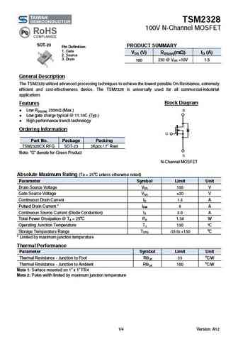
TSM2328 100V N-Channel MOSFET SOT-23 PRODUCT SUMMARY Pin Definition 1. Gate VDS (V) RDS(on)(m ) ID (A) 2. Source 3. Drain 250 @ VGS =10V 1.5 100 General Description The TSM2328 utilized advanced processing techniques to achieve the lowest possible On-Resistance, extremely efficient and cost-effectiveness device. The TSM2328 is universally used for all commercial-in... See More ⇒
9.1. Size:335K taiwansemi
tsm23n50cn.pdf 

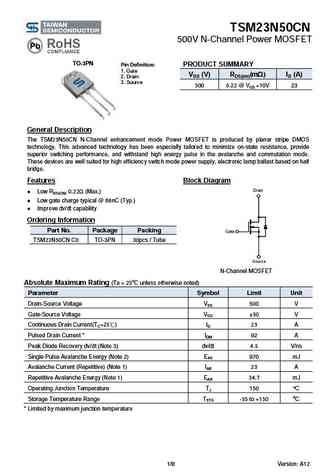
TSM23N50CN 500V N-Channel Power MOSFET TO-3PN Pin Definition PRODUCT SUMMARY 1. Gate VDS (V) RDS(on)(m ) ID (A) 2. Drain 3. Source 500 0.22 @ VGS =10V 23 General Description The TSM23N50CN N-Channel enhancement mode Power MOSFET is produced by planar stripe DMOS technology. This advanced technology has been especially tailored to minimize on-state resistance, provide ... See More ⇒
9.4. Size:208K taiwansemi
tsm2311cx.pdf 

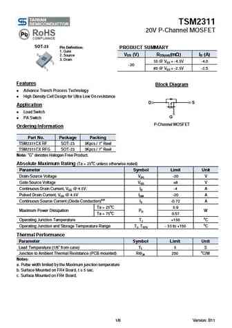
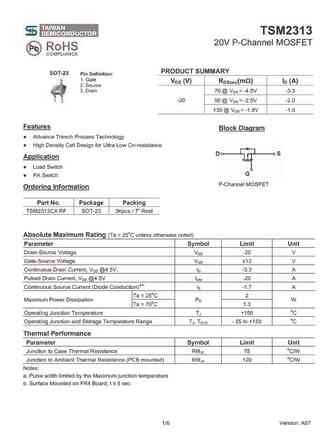
TSM2311 20V P-Channel MOSFET SOT-23 Pin Definition PRODUCT SUMMARY 1. Gate VDS (V) RDS(on)(m ) ID (A) 2. Source 3. Drain 55 @ VGS = -4.5V -4.0 -20 85 @ VGS = -2.5V -2.5 Features Block Diagram Advance Trench Process Technology High Density Cell Design for Ultra Low On-resistance Application Load Switch PA Switch P-Channel MOSFET Orderi... See More ⇒
9.5. Size:249K taiwansemi
tsm2301a.pdf 

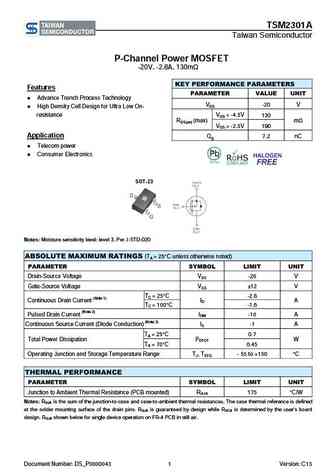
TSM2301A Taiwan Semiconductor P-Channel Power MOSFET -20V, -2.8A, 130m KEY PERFORMANCE PARAMETERS Features PARAMETER VALUE UNIT Advance Trench Process Technology VDS -20 V High Density Cell Design for Ultra Low On- resistance VGS = -4.5V 130 RDS(on) (max) m VGS = -2.5V 190 Application Qg 7.2 nC Telecom power Consumer Electronics SOT-23 ... See More ⇒
9.6. Size:195K taiwansemi
tsm2314cx.pdf 

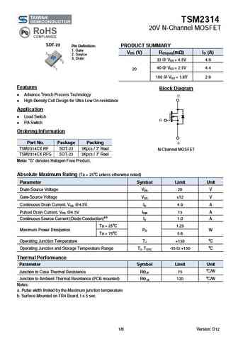
TSM2314 20V N-Channel MOSFET SOT-23 PRODUCT SUMMARY Pin Definition 1. Gate VDS (V) RDS(on)(m ) ID (A) 2. Source 3. Drain 33 @ VGS = 4.5V 4.9 40 @ VGS = 2.5V 4.4 20 100 @ VGS = 1.8V 2.9 Features Block Diagram Advance Trench Process Technology High Density Cell Design for Ultra Low On-resistance Application Load Switch PA Switch Orderin... See More ⇒
9.7. Size:238K taiwansemi
tsm2306cx.pdf 

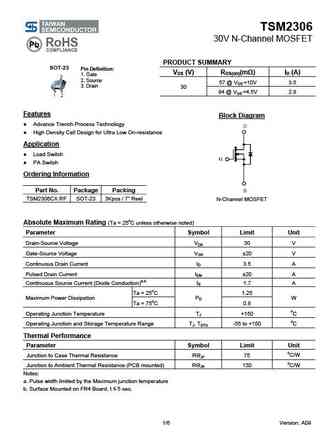
TSM2306 30V N-Channel MOSFET PRODUCT SUMMARY SOT-23 Pin Definition VDS (V) RDS(on)(m ) ID (A) 1. Gate 2. Source 57 @ VGS =10V 3.5 3. Drain 30 94 @ VGS =4.5V 2.8 Features Block Diagram Advance Trench Process Technology High Density Cell Design for Ultra Low On-resistance Application Load Switch PA Switch Ordering Information Part No. Pa... See More ⇒
9.8. Size:239K taiwansemi
tsm2310cx.pdf 

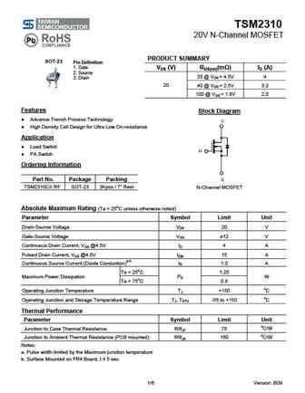
TSM2310 20V N-Channel MOSFET PRODUCT SUMMARY SOT-23 Pin Definition 1. Gate VDS (V) RDS(on)(m ) ID (A) 2. Source 33 @ VGS = 4.5V 4 3. Drain 20 40 @ VGS = 2.5V 3.2 100 @ VGS = 1.8V 2.0 Features Block Diagram Advance Trench Process Technology High Density Cell Design for Ultra Low On-resistance Application Load Switch PA Switch Ordering Info... See More ⇒
9.9. Size:213K taiwansemi
tsm2312cx.pdf 

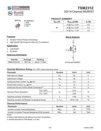
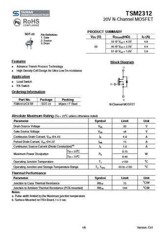
TSM2312 20V N-Channel MOSFET PRODUCT SUMMARY SOT-23 Pin Definition VDS (V) RDS(on)(m ) ID (A) 1. Gate 2. Source 33 @ VGS = 4.5V 4.9 3. Drain 20 40 @ VGS = 2.5V 4.4 51 @ VGS = 1.8V 3.9 Features Block Diagram Advance Trench Process Technology High Density Cell Design for Ultra Low On-resistance Application Load Switch PA Switch Ordering In... See More ⇒
9.11. Size:346K taiwansemi
tsm2302 a07.pdf 

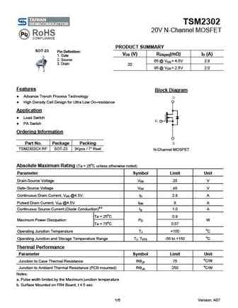
TSM2302 20V N-Channel MOSFET PRODUCT SUMMARY SOT-23 Pin Definition VDS (V) RDS(on)(m ) ID (A) 1. Gate 2. Source 65 @ VGS = 4.5V 2.8 3. Drain 20 95 @ VGS = 2.5V 2.0 Features Block Diagram Advance Trench Process Technology High Density Cell Design for Ultra Low On-resistance Application Load Switch PA Switch Ordering Information Part No.... See More ⇒
9.12. Size:186K taiwansemi
tsm2307cx.pdf 

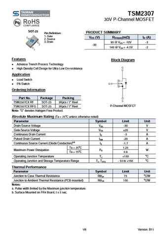
TSM2307 30V P-Channel MOSFET SOT-23 PRODUCT SUMMARY Pin Definition 1. Gate VDS (V) RDS(on)(m ) ID (A) 2. Source 3. Drain 95 @ VGS = -10V -3 -30 140 @ VGS = -4.5V -2 Features Block Diagram Advance Trench Process Technology High Density Cell Design for Ultra Low On-resistance Application Load Switch PA Switch Ordering Information Part No... See More ⇒
9.13. Size:370K taiwansemi
tsm2308cx.pdf 

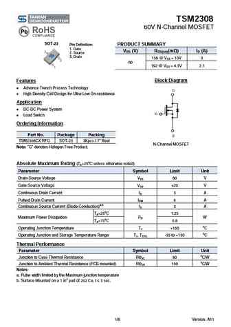
TSM2308 60V N-Channel MOSFET SOT-23 PRODUCT SUMMARY Pin Definition 1. Gate VDS (V) RDS(on)(m ) ID (A) 2. Source 3. Drain 156 @ VGS = 10V 3 60 192 @ VGS = 4.5V 2.1 Block Diagram Features Advance Trench Process Technology High Density Cell Design for Ultra Low On-resistance Application DC-DC Power System Load Switch Ordering Information ... See More ⇒
9.14. Size:357K taiwansemi
tsm2303cx.pdf 

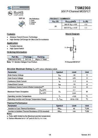
TSM2303 30V P-Channel MOSFET SOT-23 PRODUCT SUMMARY Pin Definition 1. Gate VDS (V) RDS(on)(m ) ID (A) 2. Source 3. Drain 180 @ VGS =-10V -1.3 -30 300 @ VGS =-4.5V -1.1 Block Diagram Features Advance Trench Process Technology High Density Cell Design for Ultra Low On-resistance Application Portable Devices High Speed Switch Ordering Info... See More ⇒
9.15. Size:340K taiwansemi
tsm2301acx tsm2301cx.pdf 

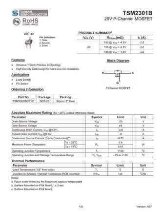
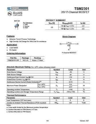
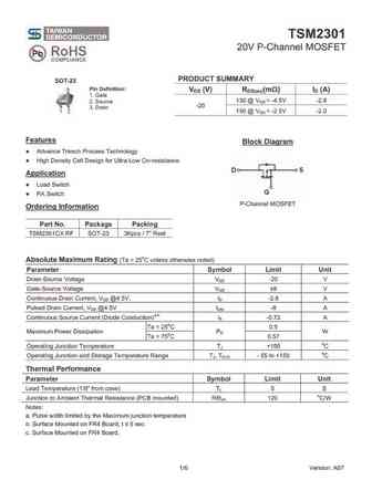
TSM2301 20V P-Channel MOSFET PRODUCT SUMMARY SOT-23 Pin Definition VDS (V) RDS(on)(m ) ID (A) 1. Gate 130 @ VGS = -4.5V -2.8 2. Source -20 3. Drain 190 @ VGS = -2.5V -2.0 Features Block Diagram Advance Trench Process Technology High Density Cell Design for Ultra Low On-resistance Application Load Switch PA Switch P-Channel MOSFET Orderi... See More ⇒
9.16. Size:315K taiwansemi
tsm2302cx.pdf 

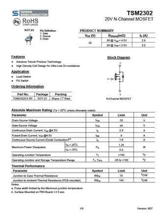
TSM2302 20V N-Channel MOSFET SOT-23 Pin Definition PRODUCT SUMMARY 1. Gate VDS (V) RDS(on)(m ) ID (A) 2. Source 3. Drain 65 @ VGS = 4.5V 2.8 20 95 @ VGS = 2.5V 2.0 Features Block Diagram Advance Trench Process Technology High Density Cell Design for Ultra Low On-resistance Application Load Switch PA Switch Ordering Information Part No.... See More ⇒
9.18. Size:237K taiwansemi
tsm2318cx.pdf 

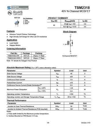
TSM2318 40V N-Channel MOSFET SOT-23 PRODUCT SUMMARY Pin Definition 1. Gate VDS (V) RDS(on)(m ) ID (A) 2. Source 3. Drain 45 @ VGS = 10V 3.9 40 62.5 @ VGS = 4.5V 3.5 Features Block Diagram Advance Trench Process Technology High Density Cell Design for Ultra Low On-resistance Application Load Switch Stepper Motors Ordering Information Pa... See More ⇒
9.19. Size:378K taiwansemi
tsm2305cx.pdf 

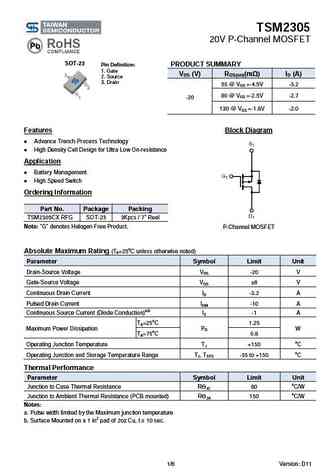
TSM2305 20V P-Channel MOSFET SOT-23 PRODUCT SUMMARY Pin Definition 1. Gate VDS (V) RDS(on)(m ) ID (A) 2. Source 3. Drain 55 @ VGS =-4.5V -3.2 80 @ VGS =-2.5V -2.7 -20 130 @ VGS =-1.8V -2.0 Block Diagram Features Advance Trench Process Technology High Density Cell Design for Ultra Low On-resistance Application Battery Management High Spe... See More ⇒
9.21. Size:912K cn vbsemi
tsm2314cx.pdf 

TSM2314CX www.VBsemi.tw N-Channel 20 V (D-S) MOSFET FEATURES PRODUCT SUMMARY Halogen-free According to IEC 61249-2-21 VDS (V) RDS(on) ( ) ID (A)e Qg (Typ.) Definition 0.028 at VGS = 4.5 V TrenchFET Power MOSFET 6a 100 % Rg Tested 20 0.042 at VGS = 2.5 V 6a 8.8 nC Compliant to RoHS Directive 2002/95/EC 0.050 at VGS = 1.8 V 5.6 APPLICATIONS DC/DC... See More ⇒
9.22. Size:911K cn vbsemi
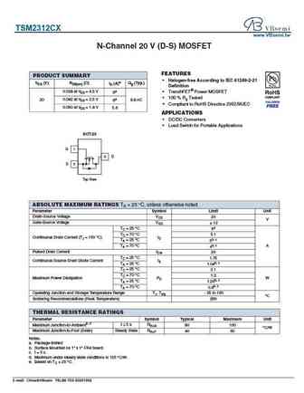
tsm2312cx.pdf 

TSM2312CX www.VBsemi.tw N-Channel 20 V (D-S) MOSFET FEATURES PRODUCT SUMMARY Halogen-free According to IEC 61249-2-21 VDS (V) RDS(on) ( ) ID (A)e Qg (Typ.) Definition 0.028 at VGS = 4.5 V TrenchFET Power MOSFET 6a 100 % Rg Tested 20 0.042 at VGS = 2.5 V 6a 8.8 nC Compliant to RoHS Directive 2002/95/EC 0.050 at VGS = 1.8 V 5.6 APPLICATIONS DC/DC... See More ⇒
Detailed specifications: TSM2307CX, TSM2308CX, TSM2310CX, TSM2311CX, TSM2312CX, TSM2313CX, TSM2314CX, TSM2318CX, AO4468, TSM2328CX, TSM23N50CN, TSM25N03CP, TSM2611EDCX6, TSM2N60CH, TSM2N60CP, TSM2N60CZ, TSM2N60SCW
Keywords - TSM2323CX MOSFET specs
TSM2323CX cross reference
TSM2323CX equivalent finder
TSM2323CX pdf lookup
TSM2323CX substitution
TSM2323CX replacement
Can't find your MOSFET?
Learn how to find a substitute transistor by analyzing voltage, current and package compatibility
