NDT455N Datasheet. Specs and Replacement
Type Designator: NDT455N 📄📄
Type of Transistor: MOSFET
Type of Control Channel: N-Channel
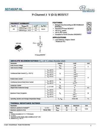
Absolute Maximum Ratings
Pd ⓘ - Maximum Power Dissipation: 3 W
|Vds|ⓘ - Maximum Drain-Source Voltage: 30 V
|Vgs|ⓘ - Maximum Gate-Source Voltage: 20 V
|Id| ⓘ - Maximum Drain Current: 11.5 A
Tj ⓘ - Maximum Junction Temperature: 150 °C
Electrical Characteristics
RDSonⓘ - Maximum Drain-Source On-State Resistance: 0.015 Ohm
Package: SOT223
📄📄 Copy
NDT455N substitution
- MOSFET ⓘ Cross-Reference Search
NDT455N datasheet
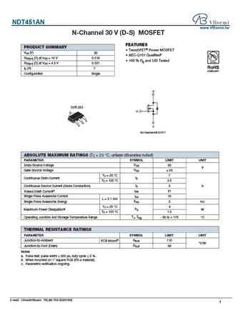
ndt451an.pdf
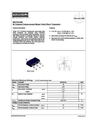
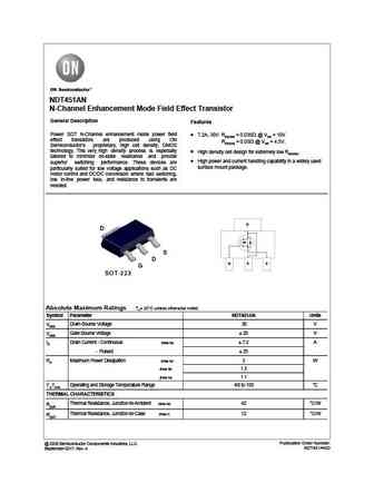
February 2009 NDT451AN N-Channel Enhancement Mode Field Effect Transistor General Description Features Power SOT N-Channel enhancement mode power field 7.2A, 30V. RDS(ON) = 0.035 @ VGS = 10V effect transistors are produced using Fairchild's RDS(ON) = 0.05 @ VGS = 4.5V. proprietary, high cell density, DMOS technology. This very high density process is especially tailored to mini... See More ⇒
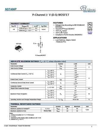
ndt456p.pdf
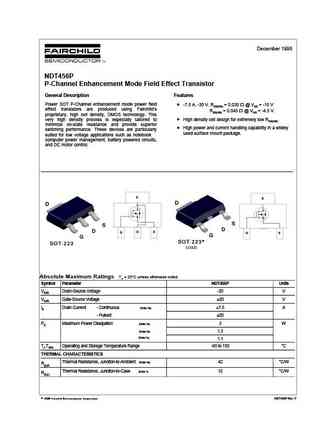
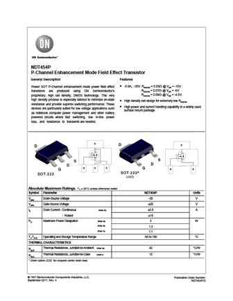
December 1998 NDT456P P-Channel Enhancement Mode Field Effect Transistor General Description Features Power SOT P-Channel enhancement mode power field -7.5 A, -30 V. RDS(ON) = 0.030 @ VGS = -10 V effect transistors are produced using Fairchild's RDS(ON) = 0.045 @ VGS = -4.5 V. proprietary, high cell density, DMOS technology. This very high density process is especially tailo... See More ⇒
ndt454p.pdf
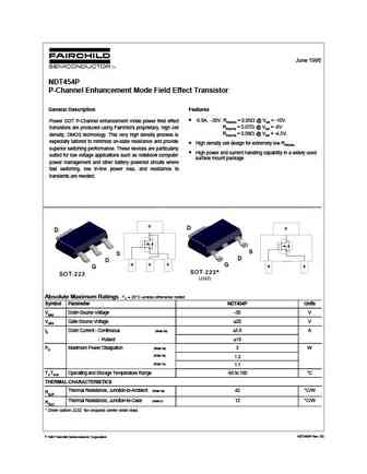
June 1996 NDT454P P-Channel Enhancement Mode Field Effect Transistor General Description Features -5.9A, -30V. RDS(ON) = 0.05 @ VGS = -10V Power SOT P-Channel enhancement mode power field effect RDS(ON) = 0.07 @ VGS = -6V transistors are produced using Fairchild's proprietary, high cell RDS(ON) = 0.09 @ VGS = -4.5V. density, DMOS technology. This very high density process is... See More ⇒
ndt452ap.pdf
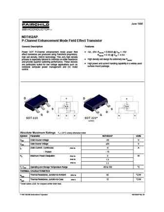
June 1996 NDT452AP P-Channel Enhancement Mode Field Effect Transistor General Description Features Power SOT P-Channel enhancement mode power field -5A, -30V. RDS(ON) = 0.065 @ VGS = -10V effect transistors are produced using Fairchild's proprietary, RDS(ON) = 0.1 @ VGS = -4.5V. high cell density, DMOS technology. This very high density process is especially tailored to minimiz... See More ⇒


Detailed specifications: NDT3055L, NDT410EL, NDT451AN, NDT451N, NDT452AP, NDT452P, NDT453N, NDT454P, IRFB4110, NDT456P, OM11N55SA, OM11N60SA, OM1N100SA, OM1N100ST, OM3N100SA, OM3N100ST, OM5N100SA
Keywords - NDT455N MOSFET specs
NDT455N cross reference
NDT455N equivalent finder
NDT455N pdf lookup
NDT455N substitution
NDT455N replacement
Need a MOSFET replacement? Our guide shows you how to find a perfect substitute by comparing key parameters and specs
MOSFET Parameters. How They Affect Each Other
History: NDT452P | NDT453N | NDT451N
🌐 : EN ES РУ

LIST
Last Update
MOSFET: MSQ60P04D | MSQ40P07D | MSQ30P40D | MSQ30P15 | MSQ30P07D | MSQ100N03D | MSHM60P14 | MSHM40N085 | MSHM30N46 | MSH60N35D
Popular searches
tip31a datasheet | d882 datasheet | tip29 transistor | s9014 transistor datasheet | 2sa1491 | 2sc1313 datasheet | 2sc984 | 2sa872