NVMFS4C05N Datasheet. Specs and Replacement
Type Designator: NVMFS4C05N
Type of Transistor: MOSFET
Type of Control Channel: N-Channel
Absolute Maximum Ratings
Pd ⓘ - Maximum Power Dissipation: 3.61 W
|Vds|ⓘ - Maximum Drain-Source Voltage: 30 V
|Vgs|ⓘ - Maximum Gate-Source Voltage: 20 V
|Id| ⓘ - Maximum Drain Current: 24.7 A
Tj ⓘ - Maximum Junction Temperature: 175 °C
Electrical Characteristics
tr ⓘ - Rise Time: 32 nS
Cossⓘ - Output Capacitance: 1215 pF
RDSonⓘ - Maximum Drain-Source On-State Resistance: 0.0034 Ohm
Package: SO-8FL
NVMFS4C05N substitution
- MOSFET ⓘ Cross-Reference Search
NVMFS4C05N datasheet
nvmfs4c05n.pdf
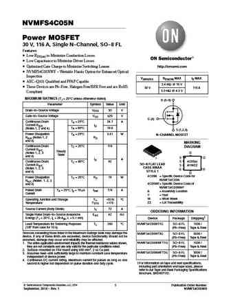
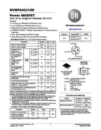
NVMFS4C05N Power MOSFET 30 V, 116 A, Single N-Channel, SO-8 FL Features Low RDS(on) to Minimize Conduction Losses Low Capacitance to Minimize Driver Losses Optimized Gate Charge to Minimize Switching Losses http //onsemi.com NVMFS4C05NWF - Wettable Flanks Option for Enhanced Optical Inspection V(BR)DSS RDS(ON) MAX ID MAX AEC-Q101 Qualified and PPAP Capable 3.4 mW ... See More ⇒
nvmfs4c03n.pdf
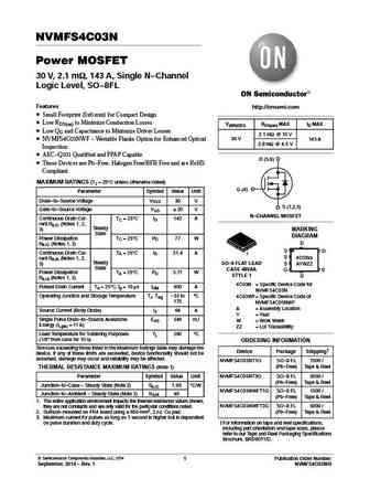
NVMFS4C03N Power MOSFET 30 V, 2.1 mW, 143 A, Single N-Channel Logic Level, SO-8FL Features http //onsemi.com Small Footprint (5x6 mm) for Compact Design Low RDS(on) to Minimize Conduction Losses V(BR)DSS RDS(on) MAX ID MAX Low QG and Capacitance to Minimize Driver Losses 2.1 mW @ 10 V 30 V NVMFS4C03NWF - Wettable Flanks Option for Enhanced Optical 143 A 2.8 mW @ 4.5 ... See More ⇒
nvmfs4c01n.pdf
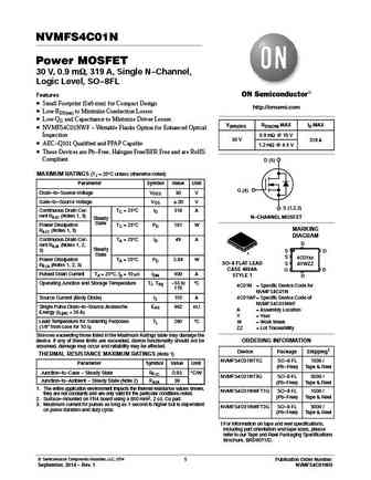
NVMFS4C01N Power MOSFET 30 V, 0.9 mW, 319 A, Single N-Channel, Logic Level, SO-8FL Features Small Footprint (5x6 mm) for Compact Design http //onsemi.com Low RDS(on) to Minimize Conduction Losses Low QG and Capacitance to Minimize Driver Losses V(BR)DSS RDS(ON) MAX ID MAX NVMFS4C01NWF - Wettable Flanks Option for Enhanced Optical 0.9 mW @ 10 V Inspection 30 V 319 A... See More ⇒
nvmfs4c302n.pdf
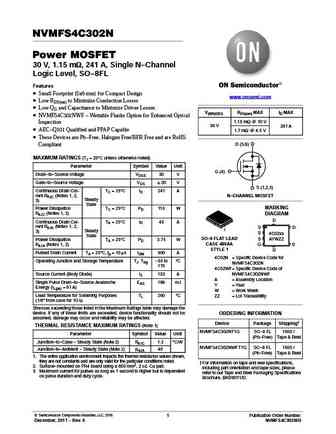
NVMFS4C302N Power MOSFET 30 V, 1.15 mW, 241 A, Single N-Channel Logic Level, SO-8FL Features Small Footprint (5x6 mm) for Compact Design www.onsemi.com Low RDS(on) to Minimize Conduction Losses Low QG and Capacitance to Minimize Driver Losses V(BR)DSS RDS(on) MAX ID MAX NVMFS4C302NWF - Wettable Flanks Option for Enhanced Optical 1.15 mW @ 10 V Inspection 30 V 241 A... See More ⇒
Detailed specifications: NVMFD5485NL, NVMFD5489NL, NVMFD5852NL, NVMFD5853N, NVMFD5853NL, NVMFD5873NL, NVMFS4C01N, NVMFS4C03N, K3569, NVMFS5113PL, NVMFS5826NL, NVMFS5830NL, NVMFS5832NL, NVMFS5833N, NVMFS5834NL, NVMFS5844NL, NVMFS5885NL
Keywords - NVMFS4C05N MOSFET specs
NVMFS4C05N cross reference
NVMFS4C05N equivalent finder
NVMFS4C05N pdf lookup
NVMFS4C05N substitution
NVMFS4C05N replacement
Need a MOSFET replacement? Our guide shows you how to find a perfect substitute by comparing key parameters and specs
🌐 : EN ES РУ

LIST
Last Update
MOSFET: ASDM30DN30E | ASDM3050KQ | ASDM2305 | ASDM2301 | ASDM2300ZA | ASDM20P13S | ASDM20N90Q | ASDM20N60 | ASDM7002EZA | ASDM68N80KQ
Popular searches
2sc2705 | bc239 | 2sc3264 | mp38a | bc546 transistor | bd243 | 2sk170 datasheet | 2n7000 equivalent