RFM12N10 Datasheet. Specs and Replacement
Type Designator: RFM12N10
Type of Transistor: MOSFET
Type of Control Channel: N-Channel
Absolute Maximum Ratings
Pd ⓘ
- Maximum Power Dissipation: 75 W
|Vds|ⓘ - Maximum Drain-Source Voltage: 100 V
|Vgs|ⓘ - Maximum Gate-Source Voltage: 20 V
|Id| ⓘ - Maximum Drain Current: 12 A
Tj ⓘ - Maximum Junction Temperature: 150 °C
Electrical Characteristics
tr ⓘ - Rise Time: 250 nS
Cossⓘ -
Output Capacitance: 300 pF
RDSonⓘ - Maximum Drain-Source On-State Resistance: 0.2 Ohm
Package: TO-204AA
- MOSFET ⓘ Cross-Reference Search
RFM12N10 datasheet
9.2. Size:175K toshiba
rfm12u7x.pdf 
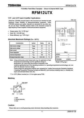
RFM12U7X TOSHIBA Field Effect Transistor Silicon N Channel MOS Type RFM12U7X VHF- and UHF-band Amplifier Applications Unit mm (Note)The TOSHIBA products listed in this document are intended for high frequency Power Amplifier of telecommunications equipment. These TOSHIBA products are neither intended nor warranted for any other use. Do not use these TOSHIBA products listed in t... See More ⇒
9.3. Size:267K fairchild semi
irfm120atf.pdf

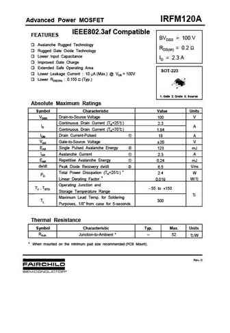
IRFM120A Advanced Power MOSFET IEEE802.3af Compatible FEATURES BVDSS = 100 V Avalanche Rugged Technology RDS(on) = 0.2 Rugged Gate Oxide Technology Lower Input Capacitance ID = 2.3 A Improved Gate Charge Extended Safe Operating Area SOT-223 Lower Leakage Current 10 A (Max.) @ VDS = 100V 2 Lower RDS(ON) 0.155 (Typ.) 1 3 1. Gate 2. Drain 3. Source Absolute Maximum ... See More ⇒
9.4. Size:269K fairchild semi
irfm120a.pdf
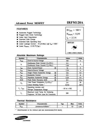
IRFM120A Advanced Power MOSFET IEEE802.3af Compatible FEATURES BVDSS = 100 V Avalanche Rugged Technology RDS(on) = 0.2 Rugged Gate Oxide Technology Lower Input Capacitance ID = 2.3 A Improved Gate Charge Extended Safe Operating Area SOT-223 Lower Leakage Current 10 A (Max.) @ VDS = 100V 2 Lower RDS(ON) 0.155 (Typ.) 1 3 1. Gate 2. Drain 3. Source Absolute Maximum ... See More ⇒
9.5. Size:965K samsung
irfm120a.pdf
Advanced Power MOSFET FEATURES BVDSS = 100 V Avalanche Rugged Technology RDS(on) = 0.2 Rugged Gate Oxide Technology Lower Input Capacitance ID = 2.3 A Improved Gate Charge Extended Safe Operating Area Lower Leakage Current 10 A (Max.) @ VDS = 100V 2 Lower RDS(ON) 0.155 (Typ.) 1 3 1. Gate 2. Drain 3. Source Absolute Maximum Ratings Symbol Characteristic Va... See More ⇒
9.6. Size:414K onsemi
irfm120a.pdf

Is Now Part of To learn more about ON Semiconductor, please visit our website at www.onsemi.com Please note As part of the Fairchild Semiconductor integration, some of the Fairchild orderable part numbers will need to change in order to meet ON Semiconductor s system requirements. Since the ON Semiconductor product management systems do not have the ability to manage part nomenclatur... See More ⇒
9.7. Size:813K cn vbsemi
irfm120a.pdf
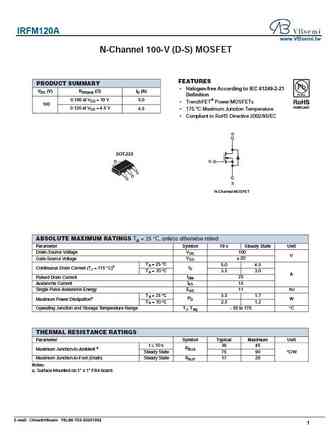
IRFM120A www.VBsemi.tw N-Channel 100-V (D-S) MOSFET FEATURES PRODUCT SUMMARY Halogen-free According to IEC 61249-2-21 VDS (V) RDS(on) ( )ID (A) Definition 0.100 at VGS = 10 V 5.0 TrenchFET Power MOSFETs 100 0.120 at VGS = 4.5 V 4.5 175 C Maximum Junction Temperature Compliant to RoHS Directive 2002/95/EC D SOT-223 D G S D G S N-Channel MOSFET ABS... See More ⇒
Detailed specifications: RFK25P08, RFK25P10, RFK35N08, RFK35N10, RFM10N12, RFM10N15, RFM12N08, RFM12N08L, 7N65, RFM12N10L, RFM12N18, RFM12N20, RFM12P08, RFM12P10, RFM15N05L, RFM15N06L, RFM15N12
Keywords - RFM12N10 MOSFET specs
RFM12N10 cross reference
RFM12N10 equivalent finder
RFM12N10 pdf lookup
RFM12N10 substitution
RFM12N10 replacement
Need a MOSFET replacement?
Our guide shows you how to find a perfect substitute by comparing key parameters and specs