UPA1917 Specs and Replacement
Type Designator: UPA1917
Type of Transistor: MOSFET
Type of Control Channel: P-Channel
Absolute Maximum Ratings
Pd ⓘ - Maximum Power Dissipation: 0.2 W
|Vds|ⓘ - Maximum Drain-Source Voltage: 20 V
|Vgs|ⓘ - Maximum Gate-Source Voltage: 8 V
|Id| ⓘ - Maximum Drain Current: 6 A
Tj ⓘ - Maximum Junction Temperature: 150 °C
Electrical Characteristics
tr ⓘ - Rise Time: 64 nS
Cossⓘ - Output Capacitance: 170 pF
RDSonⓘ - Maximum Drain-Source On-State Resistance: 0.053 Ohm
Package: SC-95
UPA1917 substitution
- MOSFET ⓘ Cross-Reference Search
UPA1917 datasheet
upa1917.pdf

To our customers, Old Company Name in Catalogs and Other Documents On April 1st, 2010, NEC Electronics Corporation merged with Renesas Technology Corporation, and Renesas Electronics Corporation took over all the business of both companies. Therefore, although the old company name remains in this document, it is a valid Renesas Electronics document. We appreciate your understanding. ... See More ⇒
upa1919.pdf

To our customers, Old Company Name in Catalogs and Other Documents On April 1st, 2010, NEC Electronics Corporation merged with Renesas Technology Corporation, and Renesas Electronics Corporation took over all the business of both companies. Therefore, although the old company name remains in this document, it is a valid Renesas Electronics document. We appreciate your understanding. ... See More ⇒
upa1912.pdf
To our customers, Old Company Name in Catalogs and Other Documents On April 1st, 2010, NEC Electronics Corporation merged with Renesas Technology Corporation, and Renesas Electronics Corporation took over all the business of both companies. Therefore, although the old company name remains in this document, it is a valid Renesas Electronics document. We appreciate your understanding. ... See More ⇒
upa1914.pdf
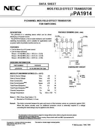
DATA SHEET MOS FIELD EFFECT TRANSISTOR PA1914 P-CHANNEL MOS FIELD EFFECT TRANSISTOR FOR SWITCHING DESCRIPTION PACKAGE DRAWING (Unit mm) The PA1914 is a switching device which can be driven +0.1 0.32 0.05 directly by a 4 V power source. 0.16+0.1 0.06 The PA1914 features a low on-state resistance and excellent switching characteristics, and is suitable for applications... See More ⇒
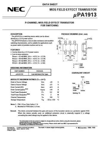
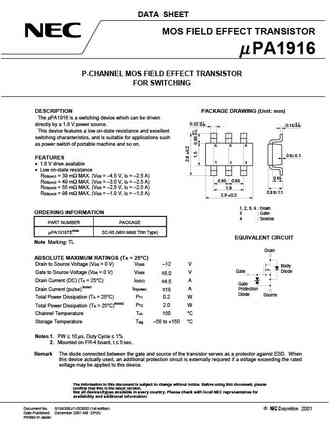
Detailed specifications: UPA1901, UPA1902, UPA1911A, UPA1912, UPA1913, UPA1914, UPA1915, UPA1916, K4145, UPA1918, UPA1919, UPA1930, UPA1931TE, UPA1932TE, UPA1950, UPA1951, UPA1952
Keywords - UPA1917 MOSFET specs
UPA1917 cross reference
UPA1917 equivalent finder
UPA1917 pdf lookup
UPA1917 substitution
UPA1917 replacement
Can't find your MOSFET? Learn how to find a substitute transistor by analyzing voltage, current and package compatibility
History: BUK7613-100E
🌐 : EN ES РУ

LIST
Last Update
MOSFET: AUN084N10 | AUN065N10 | AUN063N10 | AUN062N08BG | AUN060N08AG | AUN053N10 | AUN050N08BGL | AUN045N085 | AUN042N055 | AUN036N10
Popular searches
k3568 | 2sc1344 | cs840f | 2n3053 equivalent | 2n3569 | 2sd667 | 2sc1111 | bc239 transistor equivalent