80N06 Specs and Replacement
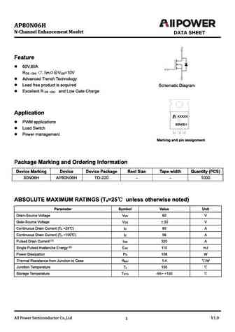
Type Designator: 80N06
Type of Transistor: MOSFET
Type of Control Channel: N-Channel
Absolute Maximum Ratings
Pd ⓘ - Maximum Power Dissipation: 150 W
|Vds|ⓘ - Maximum Drain-Source Voltage: 60 V
|Vgs|ⓘ - Maximum Gate-Source Voltage: 30 V
|Id| ⓘ - Maximum Drain Current: 80 A
Tj ⓘ - Maximum Junction Temperature: 150 °C
Electrical Characteristics
RDSonⓘ - Maximum Drain-Source On-State Resistance: 0.01 Ohm
Package: TO220C
80N06 substitution
- MOSFET ⓘ Cross-Reference Search
80N06 datasheet
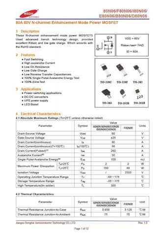
80n06 f80n06 i80n06 e80n06 b80n06 d80n06.pdf
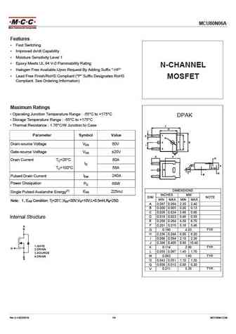
80N06/F80N06/I80N06/ E80N06/B80N06/D80N06 80A 60V N-channel Enhancement Mode Power MOSFET 1 Description These N-channel enhancement mode power MOSFETS 2 D VDS = 60V Used advanced trench technology design, provided excellent Rdson and low gate charge. Which accords with R = 7m DS(on) (Type) G the RoHS standard. 1 ID = 80A 3 S 2 Features Fast Switching High avalanche C... See More ⇒
80n06.pdf
INCHANGE Semiconductor isc N-Channel MOSFET Transistor 80N06 DESCRIPTION Drain Current I = 80A@ T =25 D C Drain Source Voltage- V = 60V(Min) DSS Fast Switching Speed 100% avalanche tested Minimum Lot-to-Lot variations for robust device performance and reliable operation APPLICATIONS General purpose power amplifier ABSOLUTE MAXIMUM RATINGS(T =25 ) C SYMBO... See More ⇒
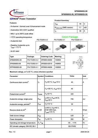
spi80n06s-08 spp80n06s-08 spb80n06s-08.pdf
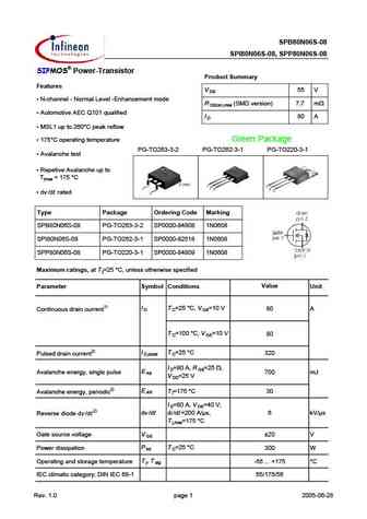
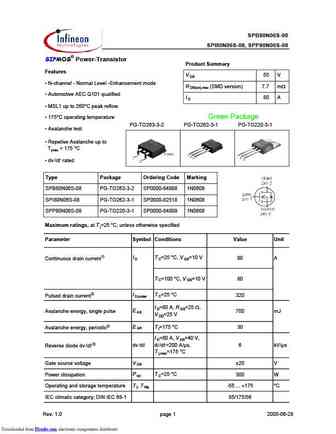
SPB80N06S-08 SPI80N06S-08, SPP80N06S-08 SIPMOS Power-Transistor Product Summary Features V 55 V DS N-channel - Normal Level -Enhancement mode R (SMD version) 7.7 m DS(on),max Automotive AEC Q101 qualified I 80 A D MSL1 up to 260 C peak reflow 175 C operating temperature Green Package PG-TO263-3-2 PG-TO262-3-1 PG-TO220-3-1 Avalanche test Repetive ... See More ⇒
phb80n06lt.pdf
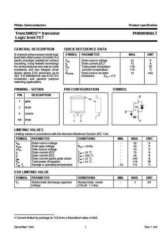
Philips Semiconductors Product specification TrenchMOS transistor PHB80N06LT Logic level FET GENERAL DESCRIPTION QUICK REFERENCE DATA N-channel enhancement mode logic SYMBOL PARAMETER MAX. UNIT level field-effect power transistor in a plastic envelope suitable for surface VDS Drain-source voltage 55 V mounting. Using trench technology ID Drain current (DC)1 75 A the device fe... See More ⇒
php80n06t 1.pdf
Philips Semiconductors Product specification TrenchMOS transistor PHP80N06T Standard level FET GENERAL DESCRIPTION QUICK REFERENCE DATA N-channel enhancement mode SYMBOL PARAMETER MAX. UNIT standard level field-effect power transistor in a plastic envelope using VDS Drain-source voltage 55 V trench technology. The device ID Drain current (DC)1 75 A features very low on-state ... See More ⇒
php80n06lt 2.pdf
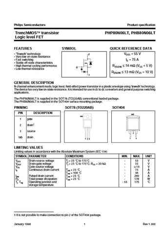
Philips Semiconductors Product specification TrenchMOS transistor PHP80N06LT, PHB80N06LT Logic level FET FEATURES SYMBOL QUICK REFERENCE DATA Trench technology VDSS = 55 V d Very low on-state resistance Fast switching ID = 75 A Stable off-state characteristics High thermal cycling performance RDS(ON) 14 m (VGS = 5 V) g Low thermal resistance ... See More ⇒
phb80n06t 1.pdf
Philips Semiconductors Product specification TrenchMOS transistor PHB80N06T Standard level FET GENERAL DESCRIPTION QUICK REFERENCE DATA N-channel enhancement mode SYMBOL PARAMETER MAX. UNIT standard level field-effect power transistor in a plastic envelope VDS Drain-source voltage 55 V suitable for surface mounting. Using ID Drain current (DC)1 75 A trench technology the devi... See More ⇒
stw80n06-10.pdf
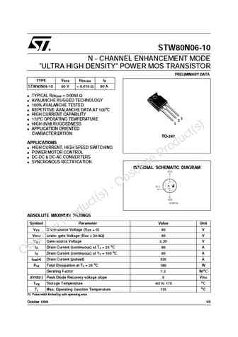
STW80N06-10 N - CHANNEL ENHANCEMENT MODE "ULTRA HIGH DENSITY" POWER MOS TRANSISTOR PRELIMINARY DATA TYPE VDSS RDS(on) ID STW80N06-10 60 V ... See More ⇒
stp80n06-10.pdf
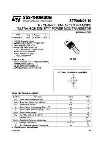
STP80N06-10 N - CHANNEL ENHANCEMENT MODE "ULTRA HIGH DENSITY" POWER MOS TRANSISTOR PRELIMINARY DATA TYPE V R I DSS DS(on) D STP80N06-10 60 V ... See More ⇒
np80n06mlg np80n06nlg np80n06plg np82n06nlg.pdf
To our customers, Old Company Name in Catalogs and Other Documents On April 1st, 2010, NEC Electronics Corporation merged with Renesas Technology Corporation, and Renesas Electronics Corporation took over all the business of both companies. Therefore, although the old company name remains in this document, it is a valid Renesas Electronics document. We appreciate your understanding. ... See More ⇒
fdp80n06.pdf
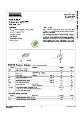
September 2007 UniFETTM FDP80N06 tm N-Channel MOSFET 60V, 80A, 10m Features Description RDS(on) = 8.5m ( Typ.)@ VGS = 10V, ID = 40A These N-Channel enhancement mode power field effect transistors are produced using Fairchild s proprietary, planar Low gate charge(Typ. 57nC) stripe, DMOS technology. Low Crss(Typ. 145pF) This advanced technology has been especially ... See More ⇒
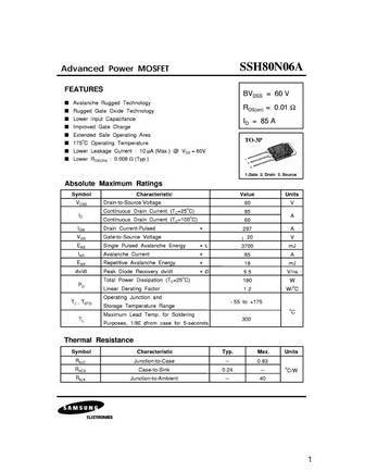
ssp80n06a.pdf
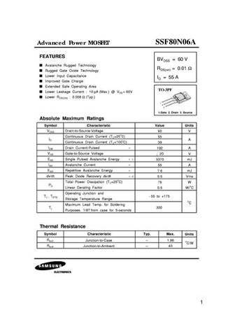
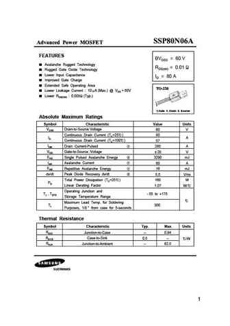
Advanced Power MOSFET FEATURES BVDSS = 60 V Avalanche Rugged Technology RDS(on) = 0.01 Rugged Gate Oxide Technology Lower Input Capacitance ID = 80 A Improved Gate Charge Extended Safe Operating Area TO-220 Lower Leakage Current 10 A (Max.) @ VDS = 60V Lower RDS(ON) 0.008 (Typ.) 1 2 3 1.Gate 2. Drain 3. Source Absolute Maximum Ratings Symbol Characteristic Value U... See More ⇒
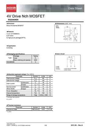
rsd080n06.pdf
Data Sheet 4V Drive Nch MOSFET RSD080N06 Structure Dimensions (Unit mm) Silicon N-channel MOSFET CPT3 6.5 (SC-63) 5.1 2.3 0.5 Features 1) Low on-resistance. 2) 4V drive. 0.75 3) High power package(CPT3). 0.65 0.9 2.3 (1) (2) (3) 2.3 0.5 1.0 Application Switching Packaging specifications Inner circuit 1 Package Taping Type Code T... See More ⇒
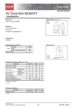
rsd080n06fra.pdf
Data Sheet AEC-Q101 Qualified 4V Drive Nch MOSFET RSD080N06 RSD080N06FRA Structure Dimensions (Unit mm) Silicon N-channel MOSFET CPT3 6.5 (SC-63) 5.1 2.3 0.5 Features 1) Low on-resistance. 2) 4V drive. 0.75 3) High power package(CPT3). 0.65 0.9 2.3 (1) (2) (3) 2.3 0.5 1.0 Application Switching Packaging specifications Inner circuit ... See More ⇒
ipp80n06s2-05 ipb80n06s2-05.pdf
IPB80N06S2-05 IPP80N06S2-05 OptiMOS Power-Transistor Product Summary Features V 55 V DS N-channel - Enhancement mode R (SMD version) 4.8 m DS(on),max Automotive AEC Q101 qualified I 80 A D MSL1 up to 260 C peak reflow 175 C operating temperature PG-TO263-3-2 PG-TO220-3-1 Green package (lead free) Ultra low Rds(on) 100% Avalanche tested Type... See More ⇒
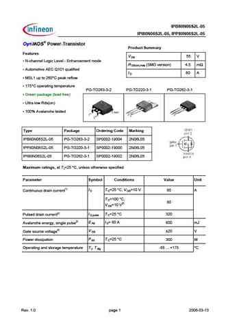
ipp80n06s2l-05 ipb80n06s2l-05 ipi80n06s2l-05.pdf
IPB80N06S2L-05 IPI80N06S2L-05, IPP80N06S2L-05 OptiMOS Power-Transistor Product Summary Features V 55 V DS N-channel Logic Level - Enhancement mode R (SMD version) 4.5 m DS(on),max Automotive AEC Q101 qualified I 80 A D MSL1 up to 260 C peak reflow 175 C operating temperature PG-TO263-3-2 PG-TO220-3-1 PG-TO262-3-1 Green package (lead free) Ultra l... See More ⇒
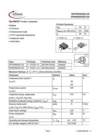
spp80n06s2-05 spb80n06s2-05.pdf
www.DataSheet4U.com SPP80N06S2-05 SPB80N06S2-05 OptiMOS Power-Transistor Product Summary Feature VDS 55 V N-Channel RDS(on) max. SMD version 4.8 m Enhancement mode ID 80 A 175 C operating temperature P- TO263 -3-2 P- TO220 -3-1 Avalanche rated dv/dt rated Type Package Ordering Code Marking SPP80N06S2-05 P- TO220 -3-1 Q67040-S4245 2N0605 SPB80N06S2-05 ... See More ⇒
spp80n06s2l-09 spb80n06s2l-09.pdf
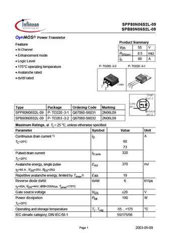
SPP80N06S2L-09 SPB80N06S2L-09 OptiMOS Power-Transistor Product Summary Feature VDS 55 V N-Channel RDS(on) 8.5 m Enhancement mode ID 80 A Logic Level P- TO263 -3-2 P- TO220 -3-1 175 C operating temperature Avalanche rated dv/dt rated Type Package Ordering Code Marking SPP80N06S2L-09 P- TO220 -3-1 Q67060-S6031 2N06L09 SPB80N06S2L-09 P- TO263 -3-2 ... See More ⇒
spp80n06s2l-h5 spb80n06s2l-h5.pdf
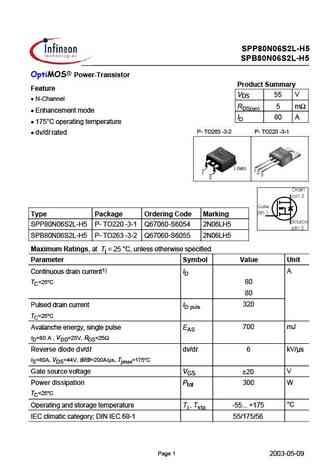
SPP80N06S2L-H5 SPB80N06S2L-H5 OptiMOS Power-Transistor Product Summary Feature VDS 55 V N-Channel RDS(on) 5 m Enhancement mode ID 80 A 175 C operating temperature P- TO263 -3-2 P- TO220 -3-1 dv/dt rated Type Package Ordering Code Marking SPP80N06S2L-H5 P- TO220 -3-1 Q67060-S6054 2N06LH5 SPB80N06S2L-H5 P- TO263 -3-2 Q67060-S6055 2N06LH5 Maximum Ratings, a... See More ⇒
ipi80n06s3-07.pdf
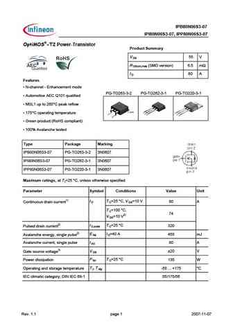
IPB80N06S3-07 IPI80N06S3-07, IPP80N06S3-07 OptiMOS -T2 Power-Transistor Product Summary V 55 V DS R (SMD version) 6.5 m DS(on),max I 80 A D Features N-channel - Enhancement mode PG-TO263-3-2 PG-TO262-3-1 PG-TO220-3-1 Automotive AEC Q101 qualified MSL1 up to 260 C peak reflow 175 C operating temperature Green product (RoHS compliant) 100% Avalanche... See More ⇒
ipb80n06s2l-11 ipp80n06s2l-11 ipi80n06s2l-11 ipp80n06s2l-11 ipb80n06s2l-11 ipi80n06s2l-11.pdf
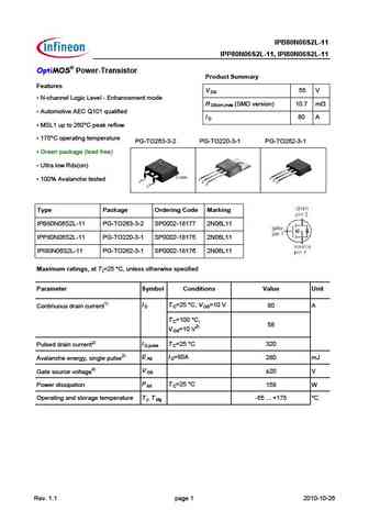
IPB80N06S2L-11 IPP80N06S2L-11, IPI80N06S2L-11 OptiMOS Power-Transistor Product Summary Features V 55 V DS N-channel Logic Level - Enhancement mode R (SMD version) 10.7 mW DS(on),max Automotive AEC Q101 qualified I 80 A D MSL1 up to 260 C peak reflow 175 C operating temperature PG-TO263-3-2 PG-TO220-3-1 PG-TO262-3-1 Green package (lead free) Ultra lo... See More ⇒
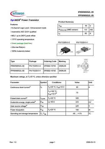
ipb80n06s2l-09 ipp80n06s2l-09 ipp80n06s2l-09 ipb80n06s2l-09.pdf
IPB80N06S2L-09 IPP80N06S2L-09 OptiMOS Power-Transistor Product Summary Features V 55 V DS N-channel Logic Level - Enhancement mode R (SMD version) 8.3 m DS(on),max Automotive AEC Q101 qualified I 80 A D MSL1 up to 260 C peak reflow 175 C operating temperature PG-TO263-3-2 PG-TO220-3-1 Green package (lead free) Ultra low Rds(on) 100% Avalanch... See More ⇒
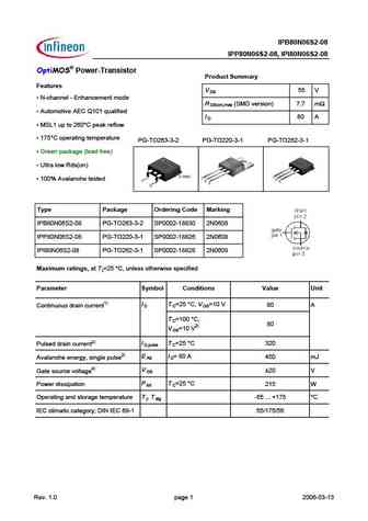
ipb80n06s2-08 ipp80n06s2-08 ipi80n06s2-08 ipp80n06s2-08 ipb80n06s2-08 ipi80n06s2-08.pdf
IPB80N06S2-08 IPP80N06S2-08, IPI80N06S2-08 OptiMOS Power-Transistor Product Summary Features V 55 V DS N-channel - Enhancement mode R (SMD version) 7.7 m DS(on),max Automotive AEC Q101 qualified I 80 A D MSL1 up to 260 C peak reflow 175 C operating temperature PG-TO263-3-2 PG-TO220-3-1 PG-TO262-3-1 Green package (lead free) Ultra low Rds(on) ... See More ⇒
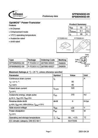
spb80n06s2-09 spp80n06s2-09.pdf
SPP80N06S2-09 Preliminary data SPB80N06S2-09 OptiMOS =Power-Transistor = == Product Summary Feature VDS 55 V N-Channel RDS(on) 9.1 m Enhancement mode ID 80 A 175 C operating temperature P-TO263-3-2 P-TO220-3-1 Avalanche rated dv/dt rated Type Package Ordering Code Marking SPP80N06S2-09 P-TO220-3-1 Q67060-S6025 2N0609 SPB80N06S2-09 P-TO263-3-2 Q67060-S6027 2N0609 Maxi... See More ⇒
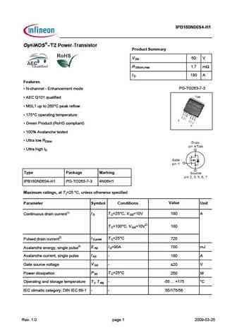
ipb180n06s4-h1 ipb180n06s4-h1 ds 10.pdf
IPB180N06S4-H1 OptiMOS -T2 Power-Transistor Product Summary V 60 V DS R 1.7 m DS(on),max I 180 A D Features PG-TO263-7-3 N-channel - Enhancement mode AEC Q101 qualified MSL1 up to 260 C peak reflow 175 C operating temperature Green Product (RoHS compliant) 100% Avalanche tested Ultra low RDSon Ultra high ID Type Package Marking IPB180N0... See More ⇒
ipi80n06s4l-05 ipp80n06s4l-05 ipb80n06s4l-05.pdf
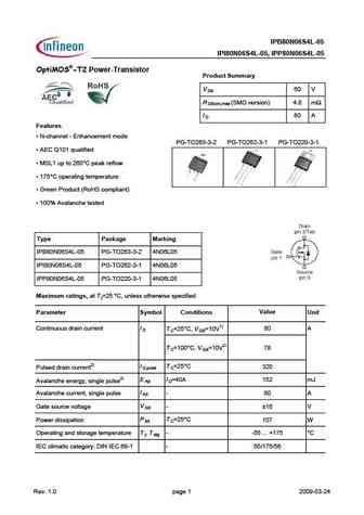
IPB80N06S4L-05 IPI80N06S4L-05, IPP80N06S4L-05 OptiMOS -T2 Power-Transistor Product Summary V 60 V DS R (SMD version) 4.8 m DS(on),max I 80 A D Features N-channel - Enhancement mode PG-TO263-3-2 PG-TO262-3-1 PG-TO220-3-1 AEC Q101 qualified MSL1 up to 260 C peak reflow 175 C operating temperature Green Product (RoHS compliant) 100% Avalanche tested... See More ⇒
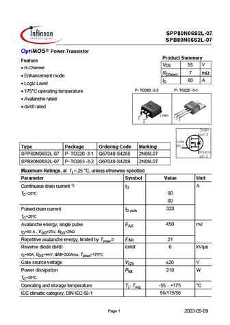
spp80n06s2l-07 spb80n06s2l-07.pdf
SPP80N06S2L-07 SPB80N06S2L-07 OptiMOS Power-Transistor Product Summary Feature VDS 55 V N-Channel RDS(on) 7 m Enhancement mode ID 80 A Logic Level P- TO263 -3-2 P- TO220 -3-1 175 C operating temperature Avalanche rated dv/dt rated Type Package Ordering Code Marking SPP80N06S2L-07 P- TO220 -3-1 Q67040-S4285 2N06L07 SPB80N06S2L-07 P- TO263 -3-2 Q6... See More ⇒
ipi80n06s4-07 ipp80n06s4-07 ipb80n06s4-07.pdf
IPB80N06S4-07 IPI80N06S4-07, IPP80N06S4-07 OptiMOS -T2 Power-Transistor Product Summary V 60 V DS R (SMD version) 7.1 m DS(on),max I 80 A D Features N-channel - Enhancement mode PG-TO263-3-2 PG-TO262-3-1 PG-TO220-3-1 AEC Q101 qualified MSL1 up to 260 C peak reflow 175 C operating temperature Green Product (RoHS compliant) 100% Avalanche tested T... See More ⇒
ipb80n06s2-07 ipp80n06s2-07 ipi80n06s2-07 ipp80n06s2-07 ipb80n06s2-07 ipi80n06s2-07.pdf
IPB80N06S2-07 IPP80N06S2-07, IPI80N06S2-07 OptiMOS Power-Transistor Product Summary Features V 55 V DS N-channel - Enhancement mode R (SMD version) 6.3 m DS(on),max Automotive AEC Q101 qualified I 80 A D MSL1 up to 260 C peak reflow 175 C operating temperature PG-TO263-3-2 PG-TO220-3-1 PG-TO262-3-1 Green package (lead free) Ultra low Rds(on) ... See More ⇒
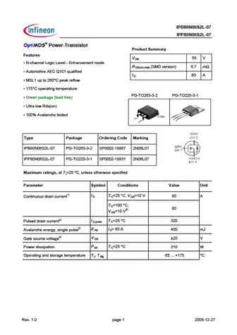
ipb80n06s2l-07 ipp80n06s2l-07 ipp80n06s2l-07 ipb80n06s2l-07.pdf
IPB80N06S2L-07 IPP80N06S2L-07 OptiMOS Power-Transistor Product Summary Features V 55 V DS N-channel Logic Level - Enhancement mode R (SMD version) 6.7 m DS(on),max Automotive AEC Q101 qualified I 80 A D MSL1 up to 260 C peak reflow 175 C operating temperature PG-TO263-3-2 PG-TO220-3-1 Green package (lead free) Ultra low Rds(on) 100% Avalanch... See More ⇒
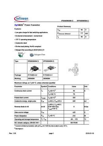
ipb080n06ng ipp080n06ng.pdf
IPB080N06N G IPP080N06N G Power-Transistor Product Summary Features V D P &?F 71C5 381A75 6?A 61BC BF9C389>7 1@@B R 7 7 m , ?> =1G ,' E5AB9?> P ( 381>>581>35=5>C >?A=1... See More ⇒
ipb80n06s4-07 ipi80n06s4-07 ipp80n06s4-07.pdf
IPB80N06S4-07 IPI80N06S4-07, IPP80N06S4-07 OptiMOS -T2 Power-Transistor Product Summary V 60 V DS R (SMD version) 7.1 m DS(on),max I 80 A D Features N-channel - Enhancement mode PG-TO263-3-2 PG-TO262-3-1 PG-TO220-3-1 AEC Q101 qualified MSL1 up to 260 C peak reflow 175 C operating temperature Green Product (RoHS compliant) 100% Avalanche tested T... See More ⇒
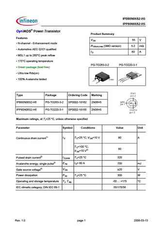
ipb80n06s2-h5 ipp80n06s2-h5 ipp80n06s2-h5 ipb80n06s2-h5.pdf
IPB80N06S2-H5 IPP80N06S2-H5 OptiMOS Power-Transistor Product Summary Features V 55 V DS N-channel - Enhancement mode R (SMD version) 5.2 m DS(on),max Automotive AEC Q101 qualified I 80 A D MSL1 up to 260 C peak reflow 175 C operating temperature PG-TO263-3-2 PG-TO220-3-1 Green package (lead free) Ultra low Rds(on) 100% Avalanche tested Type... See More ⇒
ipb80n06s3l-05.pdf
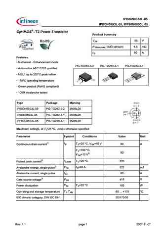
IPB80N06S3L-05 IPI80N06S3L-05, IPP80N06S3L-05 OptiMOS -T2 Power-Transistor Product Summary V 55 V DS R (SMD version) 4.5 m DS(on),max I 80 A D Features N-channel - Enhancement mode PG-TO263-3-2 PG-TO262-3-1 PG-TO220-3-1 Automotive AEC Q101 qualified MSL1 up to 260 C peak reflow 175 C operating temperature Green product (RoHS compliant) 100% Avalan... See More ⇒
spp80n06s2-08 spb80n06s2-08 spi80n06s2-08.pdf
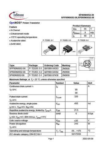
SPI80N06S2-08 SPP80N06S2-08,SPB80N06S2-08 OptiMOS Power-Transistor Product Summary Feature VDS 55 V N-Channel RDS(on) 8 m Enhancement mode ID 80 A 175 C operating temperature P- TO262 -3-1 P- TO263 -3-2 P- TO220 -3-1 Avalanche rated dv/dt rated Type Package Ordering Code Marking SPP80N06S2-08 P- TO220 -3-1 Q67060-S4283 2N0608 SPB80N06S2-08 P- TO263 -... See More ⇒
ipb80n06s4l-07 ipi80n06s4l-07 ipp80n06s4l-07 ipp80n06s4l ipb80n06s4l ipi80n06s4l-07.pdf
IPB80N06S4L-07 IPI80N06S4L-07, IPP80N06S4L-07 OptiMOS -T2 Power-Transistor Product Summary V 60 V DS R (SMD version) 6.4 m DS(on),max I 80 A D Features N-channel - Enhancement mode PG-TO263-3-2 PG-TO262-3-1 PG-TO220-3-1 AEC Q101 qualified MSL1 up to 260 C peak reflow 175 C operating temperature Green Product (RoHS compliant) 100% Avalanche tested... See More ⇒
ipb80n06s4-05 ipi80n06s4-05 ipp80n06s4-05 ipp80n06s4 ipb80n06s4 ipi80n06s4-05.pdf
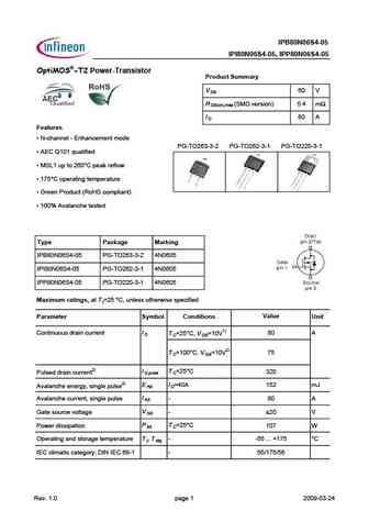
IPB80N06S4-05 IPI80N06S4-05, IPP80N06S4-05 OptiMOS -T2 Power-Transistor Product Summary V 60 V DS R (SMD version) 5.4 m DS(on),max I 80 A D Features N-channel - Enhancement mode PG-TO263-3-2 PG-TO262-3-1 PG-TO220-3-1 AEC Q101 qualified MSL1 up to 260 C peak reflow 175 C operating temperature Green Product (RoHS compliant) 100% Avalanche tested T... See More ⇒
spb80n06s-08 spi80n06s-08 spp80n06s-08 spp80n06s spb80n06s spi80n06s-08green.pdf
SPB80N06S-08 SPI80N06S-08, SPP80N06S-08 SIPMOS Power-Transistor Product Summary Features V 55 V DS N-channel - Normal Level -Enhancement mode R (SMD version) 7.7 m DS(on),max Automotive AEC Q101 qualified I 80 A D MSL1 up to 260 C peak reflow 175 C operating temperature Green Package PG-TO263-3-2 PG-TO262-3-1 PG-TO220-3-1 Avalanche test Repetive ... See More ⇒
ipp80n06s2l-h5 ipb80n06s2l-h5.pdf
IPB80N06S2L-H5 IPP80N06S2L-H5 OptiMOS Power-Transistor Product Summary Features V 55 V DS N-channel Logic Level - Enhancement mode R (SMD version) 4.7 m DS(on),max Automotive AEC Q101 qualified I 80 A D MSL1 up to 260 C peak reflow 175 C operating temperature PG-TO263-3-2 PG-TO220-3-1 Green package (lead free) Ultra low Rds(on) 100% Avalanch... See More ⇒
ipb80n06s4l-05 ipi80n06s4l-05 ipp80n06s4l-05.pdf
IPB80N06S4L-05 IPI80N06S4L-05, IPP80N06S4L-05 OptiMOS -T2 Power-Transistor Product Summary V 60 V DS R (SMD version) 4.8 m DS(on),max I 80 A D Features N-channel - Enhancement mode PG-TO263-3-2 PG-TO262-3-1 PG-TO220-3-1 AEC Q101 qualified MSL1 up to 260 C peak reflow 175 C operating temperature Green Product (RoHS compliant) 100% Avalanche tested... See More ⇒
spi80n06s-80 spp80n06s-08.pdf
SPB80N06S-08 SPI80N06S-08, SPP80N06S-08 SIPMOS Power-Transistor Product Summary Features V 55 V DS N-channel - Normal Level -Enhancement mode R (SMD version) 7.7 m DS(on),max Automotive AEC Q101 qualified I 80 A D MSL1 up to 260 C peak reflow 175 C operating temperature Green Package PG-TO263-3-2 PG-TO262-3-1 PG-TO220-3-1 Avalanche test Repetive ... See More ⇒
ipb80n06s2-09 ipp80n06s2-09 ipp80n06s2-09 ipb80n06s2-09.pdf
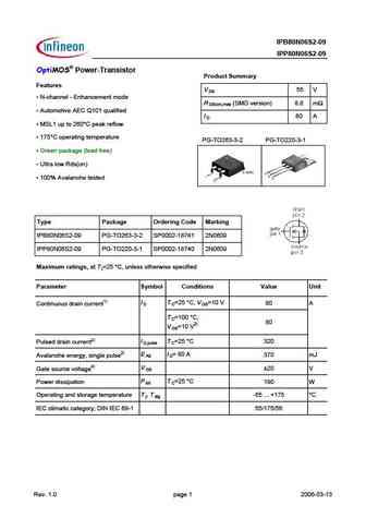
IPB80N06S2-09 IPP80N06S2-09 OptiMOS Power-Transistor Product Summary Features V 55 V DS N-channel - Enhancement mode R (SMD version) 8.8 m DS(on),max Automotive AEC Q101 qualified I 80 A D MSL1 up to 260 C peak reflow 175 C operating temperature PG-TO263-3-2 PG-TO220-3-1 Green package (lead free) Ultra low Rds(on) 100% Avalanche tested Type... See More ⇒
ipb80n06s2l-06 ipp80n06s2l-06 ipp80n06s2l-06 ipb80n06s2l-06.pdf
IPB80N06S2L-06 IPP80N06S2L-06 OptiMOS Power-Transistor Product Summary Features V 55 V DS N-channel Logic Level - Enhancement mode R (SMD version) 6.3 m DS(on),max Automotive AEC Q101 qualified I 80 A D MSL1 up to 260 C peak reflow 175 C operating temperature PG-TO263-3-2 PG-TO220-3-1 Green package (lead free) Ultra low Rds(on) 100% Avalanch... See More ⇒
utt80n06.pdf
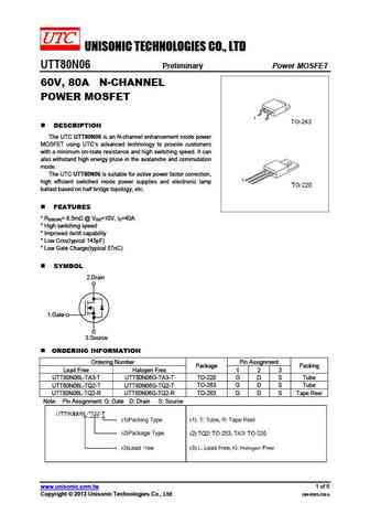
UNISONIC TECHNOLOGIES CO., LTD UTT80N06 Preliminary Power MOSFET 60V, 80A N-CHANNEL POWER MOSFET DESCRIPTION The UTC UTT80N06 is an N-channel enhancement mode power MOSFET using UTC s advanced technology to provide customers with a minimum on-state resistance and high switching speed. It can also withstand high energy pluse in the avalanche and commutation mode. The UTC U... See More ⇒
am80n06-05d.pdf
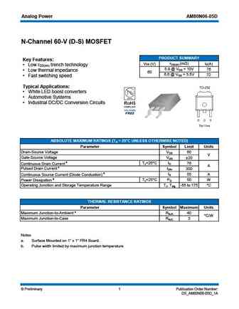
Analog Power AM80N06-05D N-Channel 60-V (D-S) MOSFET PRODUCT SUMMARY Key Features rDS(on) (m ) VDS (V) ID(A) Low r trench technology DS(on) 5.9 @ VGS = 10V 76 Low thermal impedance 60 6.6 @ VGS = 5.5V 72 Fast switching speed Typical Applications White LED boost converters Automotive Systems Industrial DC/DC Conversion Circuits ABSOLUTE MAXIM... See More ⇒
sif80n060.pdf
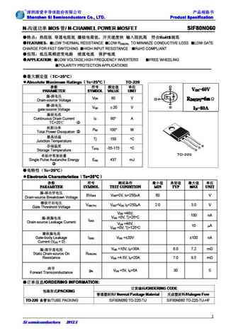
Shenzhen SI Semiconductors Co., LTD. Product Specification Shenzhen SI Semiconductors Co., LTD. Product Specification Shenzhen SI Semiconductors Co., LTD. Product Specification Shenzhen SI Semiconductors Co., LTD. Product Specification N- MOS / N-CHANNEL POWER MOSFET SIF80N060 N- MOS / N-CHANNEL POWER MOSFET SIF80N060 ... See More ⇒
g80n06 to251.pdf
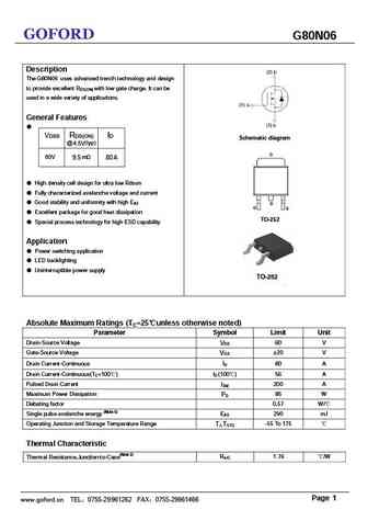
GOFORD G80N06 Description The G80N06 uses advanced trench technology and design to provide excellent R with low gate charge. It can be DS(ON) used in a wide variety of applications. General Features VDSS RDS(ON) ID Schematic diagram @ (typ) 4.5V 60V m 9.5 80 A High density cell design for ultra low Rdson Fully characterized avalanche voltage and curren... See More ⇒
g80n06 to220.pdf
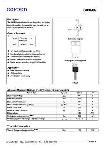
GOFORD G80N06 Description The G80N06 uses advanced trench technology and design to provide excellent R with low gate charge. It can be DS(ON) used in a wide variety of applications. General Features VDSS RDS(ON) ID Schematic diagram @ (typ) 4.5V 60V m 9.5 80 A High density cell design for ultra low Rdson Fully characterized avalanche voltage and curre... See More ⇒
80n06-251.pdf
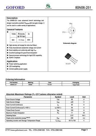
80N06-251 GOFORD Description The 80N06-251 uses advanced trench technology and design to provide excellent RDS(ON) with low gate charge. It can be used in a wide variety of applications. General Features VDSS R DS(ON) ID @ 10V (typ) 80 A 60V 11.7 m Schematic diagram High density cell design for ultra low Rdson Fully characterized avalanche voltage and cur... See More ⇒
g80n06 to252.pdf
GOFORD G80N06 Description The G80N06 uses advanced trench technology and design to provide excellent R with low gate charge. It can be DS(ON) used in a wide variety of applications. General Features VDSS RDS(ON) ID Schematic diagram @ (typ) 4.5V 60V m 9.5 80 A High density cell design for ultra low Rdson Fully characterized avalanche voltage and curre... See More ⇒
brb80n06.pdf
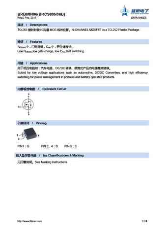
BRB80N06(BRCS80N06B) Rev.C Feb.-2015 DATA SHEET / Descriptions TO-263 N MOS N-CHANNEL MOSFET in a TO-252 Plastic Package. / Features R C DS(on) rss Low RDS(on),low gate charge, low Crss, fast switching. / Applications DC/DC ... See More ⇒
cmp80n06 cmb80n06 cmi80n06.pdf
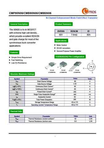
CMP80N06/CMB80N06/CMI80N06 N-Channel Enhancement Mode Field Effect Transistor General Description Product Summery The 80N06 is N-ch MOSFET BVDSS RDSON ID with extreme high cell density , 60V 7.8m 80A which provide excellent RDSON and gate charge for most of the Applications synchronous buck converter Motor Control applications. DC-DC converters General Purpose Power Amplif... See More ⇒
swha80n06v1.pdf
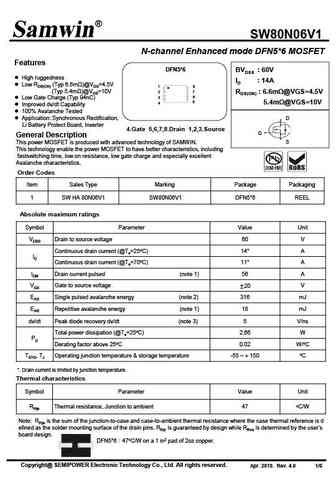
SW80N06V1 N-channel Enhanced mode DFN5*6 MOSFET Features DFN5*6 BVDSS 60V High ruggedness ID 14A Low RDS(ON) (Typ 6.6m )@VGS=4.5V 1 8 (Typ 5.4m )@VGS=10V 2 7 RDS(ON) 6.6m @VGS=4.5V 6 3 Low Gate Charge (Typ 94nC) 5 4 5.4m @VGS=10V Improved dv/dt Capability 100% Avalanche Tested Application Synchronous Rectification, D... See More ⇒
swi80n06v1.pdf
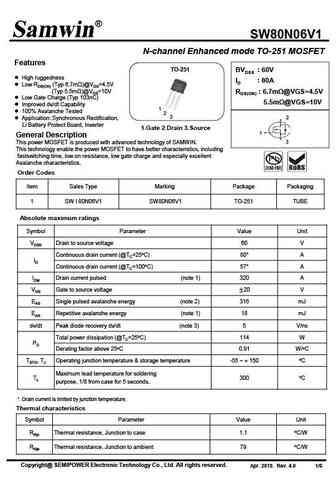
SW80N06V1 N-channel Enhanced mode TO-251 MOSFET Features TO-251 BVDSS 60V High ruggedness ID 80A Low RDS(ON) (Typ 6.7m )@VGS=4.5V (Typ 5.5m )@VGS=10V RDS(ON) 6.7m @VGS=4.5V Low Gate Charge (Typ 103nC) 5.5m @VGS=10V Improved dv/dt Capability 1 100% Avalanche Tested 2 3 2 Application Synchronous Rectification, Li Bat... See More ⇒
sre80n065fsud8.pdf
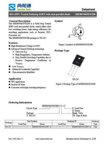
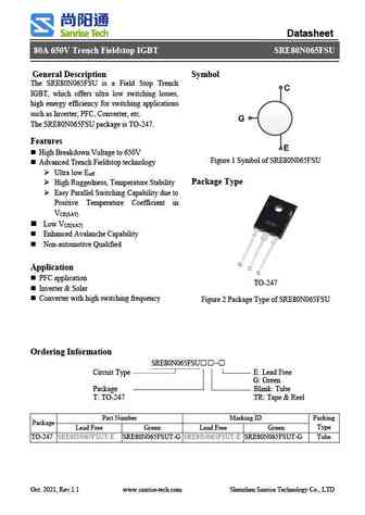
Datasheet 80A 650V Trench Fieldstop IGBT with anti-parallel diode SRE80N065FSUD8 General Description Symbol The SRE80N065FSUD8 is a Field Stop Trench IGBT with anti-parallel diode, which offers ultra low switching losses, high energy efficiency for switching applications such as Inverter, PFC, Converter, etc. The SRE80N065FSUD8 package is TO-247. Features Figure 1 Symbol o... See More ⇒
sre80n065fsu.pdf
Datasheet 80A 650V Trench Fieldstop IGBT SRE80N065FSU General Description Symbol The SRE80N065FSU is a Field Stop Trench C IGBT, which offers ultra low switching losses, high energy efficiency for switching applications such as Inverter, PFC, Converter, etc. G The SRE80N065FSU package is TO-247. Features E High Breakdown Voltage to 650V Figure 1 Symbol of SRE80N065F... See More ⇒
sre80n065fsu2.pdf
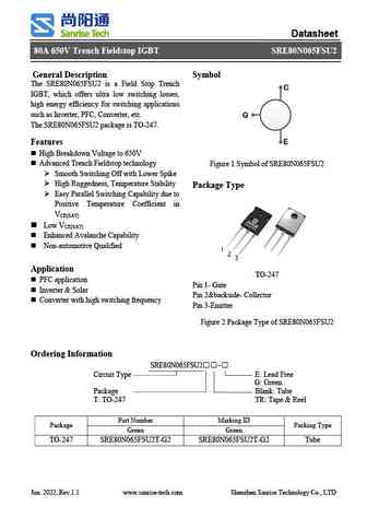
Datasheet 80A 650V Trench Fieldstop IGBT SRE80N065FSU2 General Description Symbol The SRE80N065FSU2 is a Field Stop Trench C IGBT, which offers ultra low switching losses, high energy efficiency for switching applications such as Inverter, PFC, Converter, etc. G The SRE80N065FSU2 package is TO-247. E Features High Breakdown Voltage to 650V Advanced Trench Fields... See More ⇒
sre80n065fsu2db.pdf
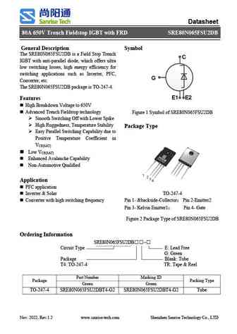
Datasheet 80A 650V Trench Fieldstop IGBT with FRD SRE80N065FSU2DB General Description Symbol The SRE80N065FSU2DB is a Field Stop Trench C IGBT with anti-parallel diode, which offers ultra low switching losses, high energy efficiency for switching applications such as Inverter, PFC, G Converter, etc. The SRE80N065FSU2DB package is TO-247-4. E1 E2 Features High Breakd... See More ⇒
sre80n065fsud6.pdf
Datasheet 80A 650V Trench Fieldstop IGBT with anti-parallel diode SRE80N065FSUD6 General Description Symbol The SRE80N065FSUD6 is a Field Stop Trench IGBT with anti-parallel diode, which offers ultra low switching losses, high energy efficiency for switching applications such as Inverter, PFC, Converter, etc. The SRE80N065FSUD6 package is TO-247. Features Figure 1 Symbol o... See More ⇒
hrlp80n06k.pdf
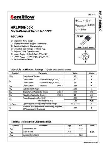
Sep 2015 BVDSS = 60 V RDS(on) typ = 6.3m HRLP80N06K ID = 80 A 60V N-Channel Trench MOSFET TO-220 FEATURES Originative New Design Superior Avalanche Rugged Technology 1 2 3 Excellent Switching Characteristics 1.Gate 2. Drain 3. Source Unrivalled Gate Charge 100 nC (Typ.) Extended Safe Operating Area Lower RDS(ON) 6.3 m (Typ.) @VG... See More ⇒
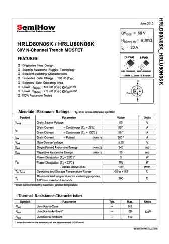
hrld80n06k hrlu80n06k.pdf
June 2015 BVDSS = 60 V RDS(on) typ HRLD80N06K / HRLU80N06K ID = 80 A 60V N-Channel Trench MOSFET D-PAK I-PAK FEATURES 2 1 Originative New Design 1 3 2 3 Superior Avalanche Rugged Technology HRLD80N06K HRLU80N06K Excellent Switching Characteristics 1.Gate 2. Drain 3. Source Unrivalled Gate Charge 100 nC (Typ.) Extended Safe Operating Area Lower RDS(ON)... See More ⇒
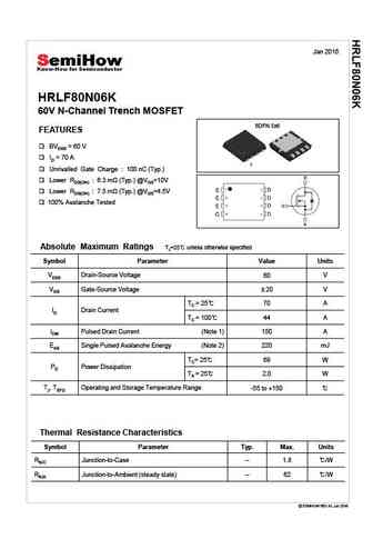
hrlf80n06k.pdf
Jan 2016 HRLF80N06K 60V N-Channel Trench MOSFET 8DFN 5x6 FEATURES BVDSS = 60 V ID = 70 A 1 Unrivalled Gate Charge 100 nC (Typ.) Lower RDS(ON) 6.3 (Typ.) @VGS=10V Lower RDS(ON) 7.5 (Typ.) @VGS=4.5V 100% Avalanche Tested Absolute Maximum Ratings TJ=25 unless otherwise specified Symbol Parameter Value Units VDSS Drain-Source Voltage 60 V VGS Gate-Source Voltage ... See More ⇒
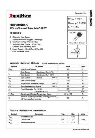
hrp80n06k.pdf
December 2014 BVDSS = 60 V RDS(on) typ = 6.3m HRP80N06K ID = 114 A 60V N-Channel Trench MOSFET TO-220 FEATURES Originative New Design Superior Avalanche Rugged Technology 1 2 3 Excellent Switching Characteristics 1.Gate 2. Drain 3. Source Unrivalled Gate Charge 90 nC (Typ.) Extended Safe Operating Area Lower RDS(ON) 6.3 m (Typ.)... See More ⇒
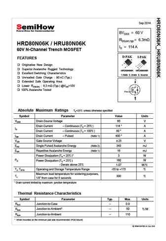
hrd80n06k hru80n06k.pdf
Sep 2014 BVDSS = 60 V RDS(on) typ HRD80N06K / HRU80N06K ID = 114 A 60V N-Channel Trench MOSFET D-PAK I-PAK FEATURES 2 1 Originative New Design 1 3 2 3 Superior Avalanche Rugged Technology HRD80N06K HRU80N06K Excellent Switching Characteristics 1.Gate 2. Drain 3. Source Unrivalled Gate Charge 90 nC (Typ.) Extended Safe Operating Area Lower RDS(ON) 6.... See More ⇒
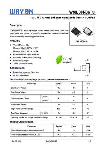
wmb80n06ts.pdf
WMB80N06TS 60V N-Channel Enhancement Mode Power MOSFET Description D D D D D D D D WMB80N06TS uses advanced power trench technology that has G been especially tailored to minimize the on-state resistance and yet ss s ss G s maintain superior switching performance. Features PDFN5060-8L V = 60V, I = 80A DS D R ... See More ⇒
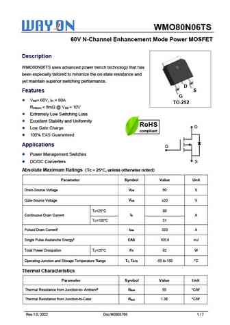
wmo80n06ts.pdf
WMO80N06TS 60V N-Channel Enhancement Mode Power MOSFET Description WMO80N06TS uses advanced power trench technology that has been especially tailored to minimize the on-state resistance and yet maintain superior switching performance. D S Features G V = 60V, I = 80A DS D TO-252 R ... See More ⇒
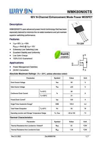
wmk80n06ts.pdf
WMK80N06TS 60V N-Channel Enhancement Mode Power MOSFET Description WMK80N06TS uses advanced power trench technology that has been especially tailored to minimize the on-state resistance and yet maintain superior switching performance. Features S D G V = 60V, I = 80A DS D TO-220 R ... See More ⇒
jmtc80n06a.pdf
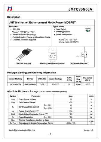
JMTC80N06A Description JMT N-channel Enhancement Mode Power MOSFET Features Application 60V, 80A Load Switch R ... See More ⇒
jmtk80n06a.pdf
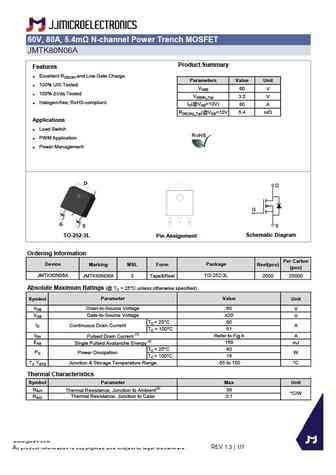
60V, 80A, 5.4m N-channel Power Trench MOSFET JMTK80N06A Product Summary Features Excellent RDS(ON) and Low Gate Charge Parameters Value Unit 100% UIS Tested VDSS 60 V 100% Vds Tested VGS(th)_Typ 3.0 V Halogen-free; RoHS-compliant ID(@VGS=10V) 80 A RDS(ON)_Typ(@VGS=10V 5.4 mW Applications Load Switch PWM Application Power Management D G S Sch... See More ⇒
jmtk480n06a.pdf
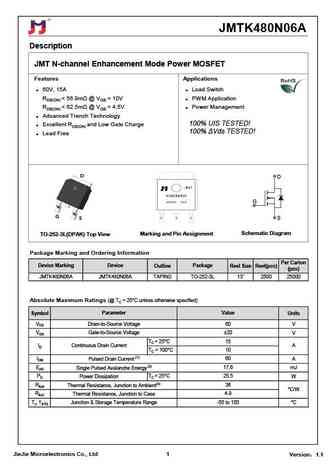
JMTK480N06A Description JMT N-channel Enhancement Mode Power MOSFET Features Applications 60V, 15A Load Switch RDS(ON) ... See More ⇒
ptp80n06 pty80n06.pdf
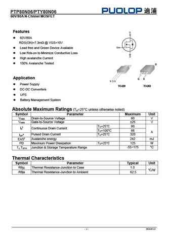
PTP80N06/PTY80N06 60V/80A N-Chnnel MOSFET Features D 60V/80A RDS(ON)=7.3m @ VGS=10V G Lead free and Green Device Available Low Rds-on to Minimize Conductive Loss S High avalanche Current % 100 Avalanche Tested D Application G S Power Supply TO-220 TO-263 DC-DC Converters UPS Battery Manageme ent System Absolute Maxim... See More ⇒
ptd80n06.pdf
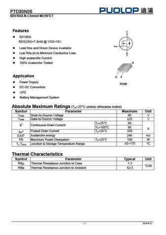
PTD80N06 60V/80A N-Chnnel MOSFET Features D 60V/80A RDS(ON)=7.3m @ VGS=10V G Lead free and Green Device Available Low Rds-on to Minimize Conductive Loss S High avalanche Current D % 100 Avalanche Tested Application G S Power Supply TO-252 DC-DC Converters UPS Battery Manageme ent System Absolute Maximum Ratings (TA=25... See More ⇒
htd480n06p.pdf
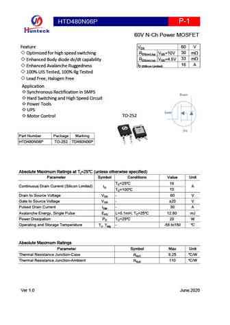
HTD480N06P P-1 60V N-Ch Power MOSFET 60 V Feature VDS 30 Optimized for high speed switching RDS(on),typ VGS=10V mW 33 RDS(on),typ VGS=4.5V mW Enhanced Body diode dv/dt capability 16 A ID (Sillicon Limited) Enhanced Avalanche Ruggedness 100% UIS Tested, 100% Rg Tested Lead Free, Halogen Free Application Synchronous Rectification in SMPS Drain Hard Swi... See More ⇒
wsf80n06h.pdf
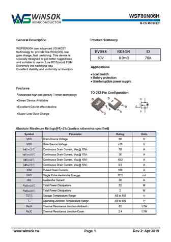
WSF80N06H N-Ch MOSFET General Description Product Summery WSF80N06H use advanced VD MOST technology to provide low RDS(ON), low BVDSS RDSON ID gate charge, fast switching This device is 60V 8.0m 70A specially designed to get better ruggedness and suitable to use in Low RDS(on) & FOM Extremely low switching loss Applications Excellent stability and uniformity or Invertors ... See More ⇒
wsr80n06.pdf
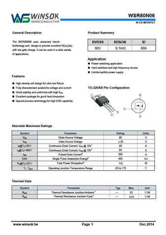
WSR80N06 N-Ch MOSFET General Description Product Summery The WSR80N06 uses advanced trench BVDSS RDSON ID technology and design to provide excellent R DS(ON) 60V 9.1m 80A with low gate charge. It can be used in a wide variety of applications. Application Power switching application Hard switched and high frequency circuits Uninterruptible power supply Feature... See More ⇒
vsi080n06ms.pdf
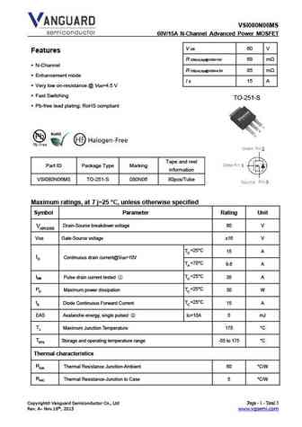
VSI080N06MS 60V/15A N-Channel Advanced Power MOSFET V DS 60 V Features R DS(on),typ@VGS=10V 68 m N-Channel R DS(on),typ@VGS=4.5V 85 m Enhancement mode I D 15 A Very low on-resistance @ VGS=4.5 V Fast Switching TO-251-S Pb-free lead plating; RoHS compliant Tape and reel Part ID Package Type Marking information VSI080N06MS TO-251-S 080N06 8... See More ⇒
vbzl80n06.pdf
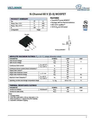
VBZL80N06 www.VBsemi.com N-Channel 60 V (D-S) MOSFET FEATURES PRODUCT SUMMARY TrenchFET power MOSFET VDS 60 V Package with low thermal resistance RDS(on) VGS = 10 V 6 m AEC-Q101 qualified d RDS(on) VGS = 4.5 V 11 m 100 % Rg and UIS tested ID 100 A Configuration Single TO-263 D G S S D D G G N-Channel MOSFET S Top View ABSOLUTE MAXIMUM RATINGS ... See More ⇒
vbze80n06.pdf
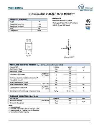
VBZE80N06 www.VBsemi.com N-Channel 60 V (D-S) 175 C MOSFET FEATURES PRODUCT SUMMARY TrenchFET Power MOSFET VDS (V) 60 Package with Low Thermal Resistance RDS(on) ( ) at VGS = 10 V 0.006 100 % Rg and UIS Tested RDS(on) ( ) at VGS = 4.5 V 0.008 100 ID (A) Single Configuration D TO-252 G G D S S Top View N-Channel MOSFET ABSOLUTE MAXIMUM RATINGS (TC = 25... See More ⇒
vbzm80n06.pdf
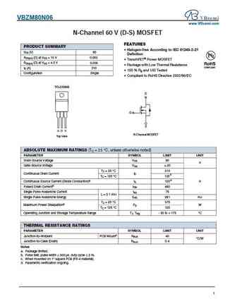
VBZM80N06 www.VBsemi.com N-Channel 60 V (D-S) MOSFET FEATURES PRODUCT SUMMARY Halogen-free According to IEC 61249-2-21 VDS (V) 60 Definition RDS(on) ( ) at VGS = 10 V 0.003 TrenchFET Power MOSFET RDS(on) ( ) at VGS = 4.5 V 0.009 Package with Low Thermal Resistance ID (A) 210 100 % Rg and UIS Tested Configuration Single Compliant to RoHS Directive 2002/9... See More ⇒
ipp80n06s2l-07.pdf
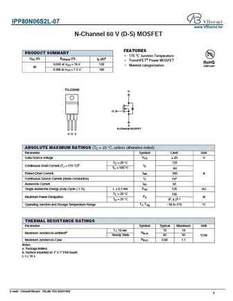
IPP80N06S2L-07 www.VBsemi.tw N-Channel 60 V (D-S) MOSFET FEATURES PRODUCT SUMMARY 175 C Junction Temperature VDS (V) RDS(on) ( ) ID (A)a TrenchFET Power MOSFET 0.005 at VGS = 10 V 120 Material categorization 60 0.008 at VGS = 7.5 V 100 TO-220AB D G S N-Channel MOSFET G D S ABSOLUTE MAXIMUM RATINGS (TC = 25 C, unless otherwise noted) Parameter Symbol Li... See More ⇒
hm80n06k.pdf
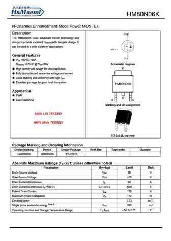
N-Channel Enhancement Mode Power MOSFET Description The uses advanced trench technology and design to provide excellent RDS(ON) with low gate charge. It can be used in a wide variety of applications. General Features VDS =60V,ID =80A RDS(ON) ... See More ⇒
hms80n06d.pdf
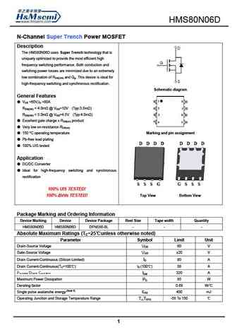
N-Channel Super Trench Power MOSFET Description The HMS80N06D uses Super Trench technology that is uniquely optimized to provide the most efficient high frequency switching performance. Both conduction and switching power losses are minimized due to an extremely low combination of R and Q . This device is ideal for DS(ON) g high-frequency switching and synchronous rec... See More ⇒
hm80n06ka.pdf
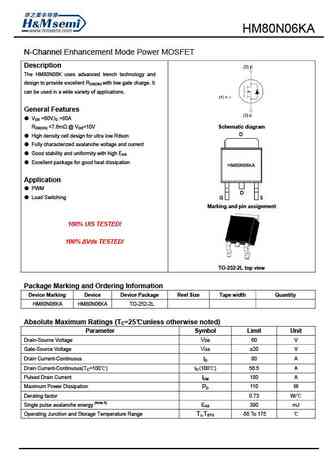
HM80N06KA N-Channel Enhancement Mode Power MOSFET Description The HM80N06K uses advanced trench technology and design to provide excellent RDS(ON) with low gate charge. It can be used in a wide variety of applications. General Features VDS =60V,ID =80A RDS(ON) ... See More ⇒
mpg80n06p mdt80n06d.pdf
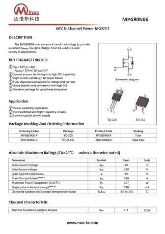
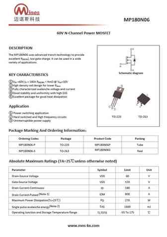
60V N-Channel Power MOSFET DESCRIPTION The MPG80N06 uses advanced trench technology to provide excellent R , low gate charge. It can be used in a wide DS(ON) variety of applications. KEY CHARACTERISTICS V = 60V,I = 80A DS D R ... See More ⇒
mdt80n06d.pdf
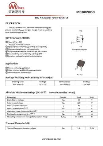
60V N-Channel Power MOSFET DESCRIPTION The MDT80N06D uses advanced trench technology to provide excellent R , low gate charge. It can be used in a DS(ON) wide variety of applications. KEY CHARACTERISTICS V = 60V,I = 80A DS D R ... See More ⇒
mp180n06p mp180n06p.pdf
60V N-Channel Power MOSFET DESCRIPTION The MP180N06 uses advanced trench technology to provide excellent R ), low gate charge. It can be used in a wide DS(ON variety of applications. Schematic diagram KEY CHARACTERISTICS V =60V,I = 180A R ... See More ⇒
ipp80n06s2-09.pdf
isc N-Channel MOSFET Transistor IPP80N06S2-09 FEATURES Drain Current I = 100A@ T =25 D C Drain Source Voltage- V = 55V(Min) DSS Static Drain-Source On-Resistance R 9.1m (Max) DS(on) 100% avalanche tested Minimum Lot-to-Lot variations for robust device performance and reliable operation DESCRITION Ultra Low On-resistance Fast Switching Type Marking ... See More ⇒
ap80n06d.pdf
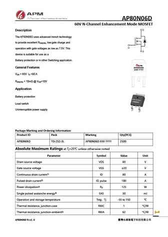
AP80N06D 60V N-Channel Enhancement Mode MOSFET Description The AP80N06D uses advanced trench technology to provide excellent R , low gate charge and DS(ON) operation with gate voltages as low as 7.5V. This device is suitable for use as a Battery protection or in other Switching application. General Features V = 60V I =80 A DS D R ... See More ⇒
ap80n06nf.pdf
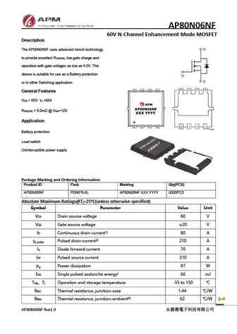
AP80N06NF 60V N-Channel Enhancement Mode MOSFET Description The AP80N06NF uses advanced trench technology to provide excellent R , low gate charge and DS(ON) operation with gate voltages as low as 4.5V. This device is suitable for use as a Battery protection or in other Switching application. General Features V = 60V I =80A DS D R ... See More ⇒
Detailed specifications: NTGD3148NT1G, 2SK1085-M, 2SK1969-01, 2SK2258, 2SK2753, 2SK3262, 2SK428, 30N50, AO4407, AM30N10, AOD2144, BUK437-500B, BUK637-500B, CSD30N30, FCH067N65S3, FCP067N65S3, FCP099N65S3
Keywords - 80N06 MOSFET specs
80N06 cross reference
80N06 equivalent finder
80N06 pdf lookup
80N06 substitution
80N06 replacement
Need a MOSFET replacement? Our guide shows you how to find a perfect substitute by comparing key parameters and specs
History: IRF833FI | AOC3864 | SM2604NSC | NTR1P02LT1G | AUIRF7342Q | SI1539CDL-T1 | IRF7379Q
🌐 : EN ES РУ
LIST
Last Update
MOSFET: AUB034N10 | AUB033N08BG | AUB026N085 | AUA062N08BG | AUA060N08AG | AUA056N08BGL | AUA039N10 | ASW80R290E | ASW65R120EFD | ASW65R110E
Popular searches
bc546 datasheet | mpsa06 transistor | tta004b | 2sc1116 | 2n3565 equivalent | 10n60 | 2sc1061 | a1023
