7N60AF Specs and Replacement
Type Designator: 7N60AF
Type of Transistor: MOSFET
Type of Control Channel: N-Channel
Absolute Maximum Ratings
Pd ⓘ
- Maximum Power Dissipation: 48 W
|Vds|ⓘ - Maximum Drain-Source Voltage: 600 V
|Vgs|ⓘ - Maximum Gate-Source Voltage: 30 V
|Id| ⓘ - Maximum Drain Current: 7 A
Tj ⓘ - Maximum Junction Temperature: 150 °C
Electrical Characteristics
tr ⓘ - Rise Time: 170 nS
Cossⓘ -
Output Capacitance: 180 pF
RDSonⓘ - Maximum Drain-Source On-State Resistance: 1 Ohm
Package: TO-220F
- MOSFET ⓘ Cross-Reference Search
7N60AF datasheet
..1. Size:653K nell
7n60af 7n60h.pdf 
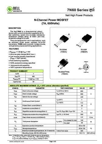
RoHS 7N60 Series RoHS SEMICONDUCTOR Nell High Power Products N-Channel Power MOSFET (7A, 600Volts) DESCRIPTION The Nell 7N60 is a three-terminal silicon device with current conduction capability of 7A, D fast switching speed, low on-state resistance, breakdown voltage rating of 600V ,and max. threshold voltage of 4 volts. They are designed for use in applications. such as sw... See More ⇒
9.5. Size:173K fairchild semi
hgtp7n60a4 hgtg7n60a4 hgt1s7n60a4.pdf
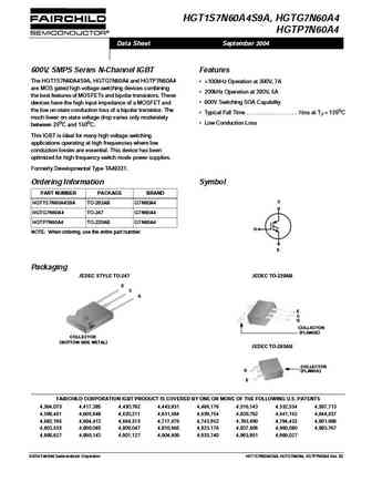
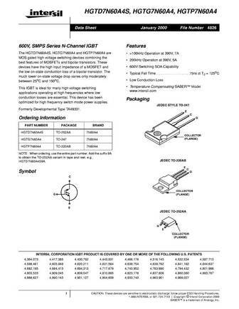
HGT1S7N60A4S9A, HGTG7N60A4 HGTP7N60A4 Data Sheet September 2004 600V, SMPS Series N-Channel IGBT Features The HGT1S7N60A4S9A, HGTG7N60A4 and HGTP7N60A4 >100kHz Operation at 390V, 7A are MOS gated high voltage switching devices combining 200kHz Operation at 390V, 5A the best features of MOSFETs and bipolar transistors. These 600V Switching SOA Capability devices have t... See More ⇒
9.6. Size:505K samsung
ssw7n60a.pdf
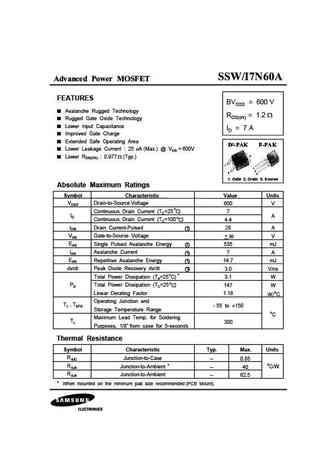
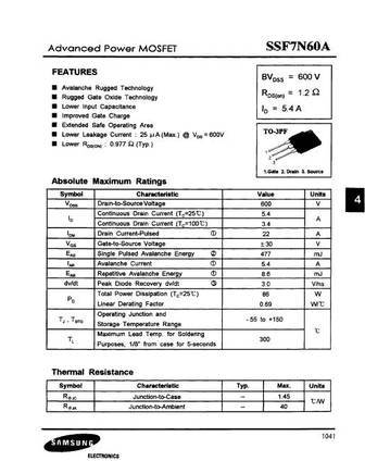
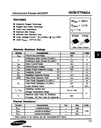
Advanced Power MOSFET FEATURES BVDSS = 600 V Avalanche Rugged Technology RDS(on) = 1.2 Rugged Gate Oxide Technology Lower Input Capacitance ID = 7 A Improved Gate Charge Extended Safe Operating Area Lower Leakage Current 25 A (Max.) @ VDS = 600V 2 Lower RDS(ON) 0.977 (Typ.) 1 1 2 3 3 1. Gate 2. Drain 3. Source Absolute Maximum Ratings Symbol Chara... See More ⇒
9.7. Size:912K samsung
ssh7n60a.pdf

Advanced Power MOSFET FEATURES BVDSS = 600 V Avalanche Rugged Technology RDS(on) = 1.2 Rugged Gate Oxide Technology Lower Input Capacitance ID = 7.3 A Improved Gate Charge Extended Safe Operating Area Lower Leakage Current 25 A (Max.) @ VDS = 600V Lower RDS(ON) 0.977 (Typ.) 1 2 3 1.Gate 2. Drain 3. Source Absolute Maximum Ratings Symbol Characteristic Va... See More ⇒
9.8. Size:581K samsung
ssp7n60a.pdf
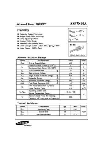
Advanced Power MOSFET FEATURES BVDSS = 600 V Avalanche Rugged Technology RDS(on) = 1.2 Rugged Gate Oxide Technology Lower Input Capacitance ID = 7 A Improved Gate Charge Extended Safe Operating Area Lower Leakage Current 25 A (Max.) @ VDS = 600V Lower RDS(ON) 0.977 (Typ.) 1 2 3 1.Gate 2. Drain 3. Source Absolute Maximum Ratings Symbol Characteristic Valu... See More ⇒
9.9. Size:944K samsung
ssh17n60a.pdf
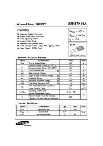
Advanced Power MOSFET FEATURES BVDSS = 600 V Avalanche Rugged Technology RDS(on) = 0.45 Rugged Gate Oxide Technology Lower Input Capacitance ID = 17 A Improved Gate Charge Extended Safe Operating Area Lower Leakage Current 25 A (Max.) @ VDS = 600V Lower RDS(ON) 0.356 (Typ.) 1 2 3 1.Gate 2. Drain 3. Source Absolute Maximum Ratings Symbol Characteristic Va... See More ⇒
9.10. Size:504K samsung
sss7n60a.pdf
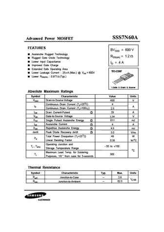
Advanced Power MOSFET FEATURES BVDSS = 600 V Avalanche Rugged Technology RDS(on) = 1.2 Rugged Gate Oxide Technology Lower Input Capacitance ID = 4 A Improved Gate Charge Extended Safe Operating Area Lower Leakage Current 25 A (Max.) @ VDS = 600V Lower RDS(ON) 0.977 (Typ.) 1 2 3 1.Gate 2. Drain 3. Source Absolute Maximum Ratings Symbol Characteristic Valu... See More ⇒
9.11. Size:171K vishay
sihg47n60aef.pdf
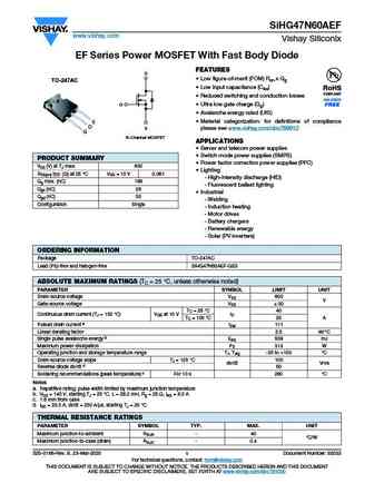
SiHG47N60AEF www.vishay.com Vishay Siliconix EF Series Power MOSFET With Fast Body Diode FEATURES D Low figure-of-merit (FOM) Ron x Qg TO-247AC Low input capacitance (Ciss) Reduced switching and conduction losses G Ultra low gate charge (Qg) Avalanche energy rated (UIS) Material categorization for definitions of compliance S D S please see www.vishay.com... See More ⇒
9.12. Size:242K onsemi
hgt1s7n60a4s9a hgtg7n60a4 hgtp7n60a4.pdf
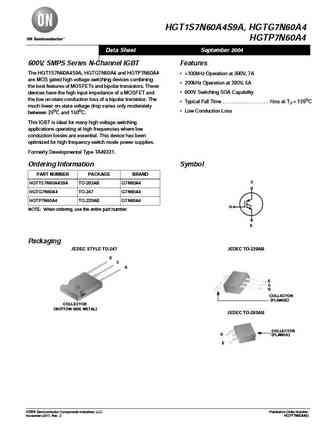
HGT1S7N60A4S9A, HGTG7N60A4 HGTP7N60A4 Data Sheet September 2004 600V, SMPS Series N-Channel IGBT Features The HGT1S7N60A4S9A, HGTG7N60A4 and HGTP7N60A4 >100kHz Operation at 390V, 7A are MOS gated high voltage switching devices combining 200kHz Operation at 390V, 5A the best features of MOSFETs and bipolar transistors. These 600V Switching SOA Capability devices have t... See More ⇒
9.13. Size:537K onsemi
hgtg7n60a4d hgtp7n60a4d hgt1s7n60a4ds.pdf
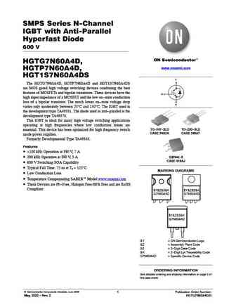
SMPS Series N-Channel IGBT with Anti-Parallel Hyperfast Diode 600 V HGTG7N60A4D, www.onsemi.com HGTP7N60A4D, HGT1S7N60A4DS The HGTG7N60A4D, HGTP7N60A4D and HGT1S7N60A4DS are MOS gated high voltage switching devices combining the best features of MOSFETs and bipolar transistors. These devices have the high input impedance of a MOSFET and the low on-state conduction loss of a bipolar ... See More ⇒
9.14. Size:260K utc
7n60a.pdf
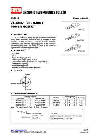
UNISONIC TECHNOLOGIES CO., LTD 7N60A Power MOSFET 7A, 600V N-CHANNEL POWER MOSFET DESCRIPTION The UTC 7N60A is a high voltage N-Channel enhancement mode power field effect transistors and is designed to have minimize on-state resistance , provide superior switching performance, and withstand high energy pulse in the avalanche and commutation mode. This power MOSFET is well sui... See More ⇒
9.15. Size:243K inpower semi
fsa07n60a.pdf
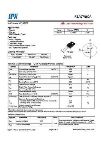
FSA07N60A N-Channel MOSFET Pb Lead Free Package and Finish Applications VDSS RDS(ON) (Max.) ID Adaptor Charger 600 V 1.25 7.0 A SMPS Standby Power Features RoHS Compliant Low ON Resistance Low Gate Charge Peak Current vs Pulse Width Curve ESD improved Capability G DS TO-220F Ordering Information PART NUMBER PACKAGE BRAND Packages FSA07N6... See More ⇒
9.16. Size:598K belling
bl7n60a-p bl7n60a-a bl7n60a-u bl7n60a-d.pdf
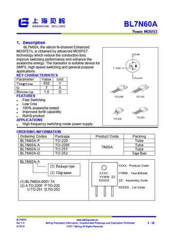
BL7N60A Power MOSFET Power MOSFET Power MOSFET Power MOSFET 1 Description BL7N60A, the silicon N-channel Enhanced MOSFETs, is obtained by advanced MOSFET technology which reduce the conduction loss, improve switching performance and enhance the avalanche energy. The transistor is suitable device for SMPS, high speed switching and general purpose application... See More ⇒
9.17. Size:1020K feihonltd
fhp7n60a fhf7n60a.pdf
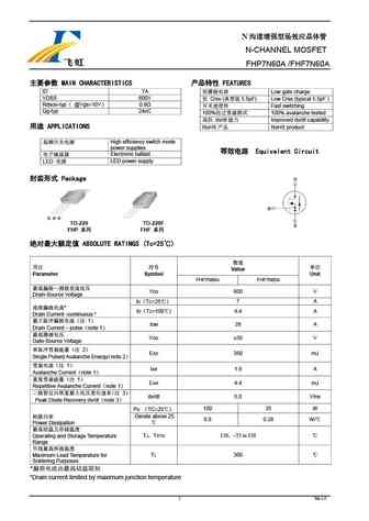
N N-CHANNEL MOSFET FHP7N60A /FHF7N60A MAIN CHARACTERISTICS FEATURES ID 7A Low gate charge VDSS 600V Crss ( 5.5pF) Low Crss (typical 5.5pF ) Rdson-typ @Vgs=10V 0.9 Fast switching Qg-typ 24nC 100% 100% avalanche tested dv/dt Impr... See More ⇒
9.18. Size:348K wuxi china
cs7n60a7hd.pdf
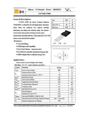
Silicon N-Channel Power MOSFET R CS7N60 A7HD General Description VDSS 600 V CS7N60 A7HD, the silicon N-channel Enhanced ID 7 A PD(TC=25 ) 40 W VDMOSFETs, is obtained by the self-aligned planar Technology RDS(ON)Typ 0.88 which reduce the conduction loss, improve switching performance and enhance the avalanche energy. The transistor can be used in various pow... See More ⇒
9.19. Size:352K wuxi china
cs7n60a8hd.pdf
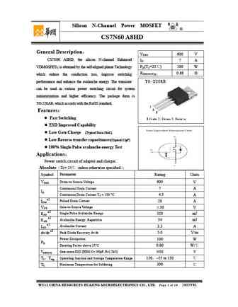
Silicon N-Channel Power MOSFET R CS7N60 A8HD General Description VDSS 600 V CS7N60 A8HD, the silicon N-channel Enhanced ID 7 A PD(TC=25 ) 100 W VDMOSFETs, is obtained by the self-aligned planar Technology RDS(ON)Typ 0.88 which reduce the conduction loss, improve switching performance and enhance the avalanche energy. The transistor can be used in various pow... See More ⇒
9.20. Size:1052K cn hmsemi
hms47n60a.pdf
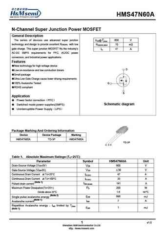
HMS47N60A N-Channel Super Junction Power MOSFET General Description The series of devices use advanced super junction 600 V VDS@Tjmax technology and design to provide excellent RDS(ON) with low RDS(ON) MAX 70 m gate charge. This super junction MOSFET fits the industry s ID A AC-DC SMPS requirements for PFC, AC/DC power conversion, and industrial power applications. Fea... See More ⇒
9.21. Size:261K inchange semiconductor
sihg47n60aef.pdf
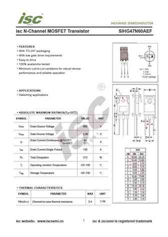
isc N-Channel MOSFET Transistor SIHG47N60AEF FEATURES With TO-247 packaging With low gate drive requirements Easy to drive 100% avalanche tested Minimum Lot-to-Lot variations for robust device performance and reliable operation APPLICATIONS Switching applications ABSOLUTE MAXIMUM RATINGS(T =25 ) a SYMBOL PARAMETER VALUE UNIT V Drain-Source Voltage 600 V DSS V ... See More ⇒
Detailed specifications: 6N80AF, 6N90A, 6N90AF, 75N08, 75N10A, 75N10B, MSAFA75N10C, MSAFX76N07A, IRFB31N20D, 7N60H, 7N90A, 7N90AF, 8N60H, 8N80A, 8N80AF, 8N80B, MSAEX8P50A
Keywords - 7N60AF MOSFET specs
7N60AF cross reference
7N60AF equivalent finder
7N60AF pdf lookup
7N60AF substitution
7N60AF replacement
Step-by-step guide to finding a MOSFET replacement. Cross-reference parts and ensure compatibility for your repair or project.