DMN1019UVT Datasheet. Specs and Replacement
Type Designator: DMN1019UVT 📄📄
Type of Transistor: MOSFET
Type of Control Channel: N-Channel
Absolute Maximum Ratings
Pd ⓘ - Maximum Power Dissipation: 1.73 W
|Vds|ⓘ - Maximum Drain-Source Voltage: 12 V
|Vgs|ⓘ - Maximum Gate-Source Voltage: 8 V
|Id| ⓘ - Maximum Drain Current: 10.7 A
Tj ⓘ - Maximum Junction Temperature: 150 °C
Electrical Characteristics
tr ⓘ - Rise Time: 3.7 nS
Cossⓘ - Output Capacitance: 415 pF
RDSonⓘ - Maximum Drain-Source On-State Resistance: 0.01 Ohm
Package: TSOT26
📄📄 Copy
- MOSFET ⓘ Cross-Reference Search
DMN1019UVT datasheet
..1. Size:310K diodes
dmn1019uvt.pdf 
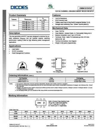
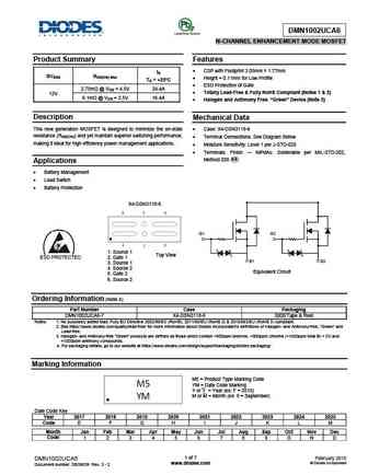
DMN1019UVT 12V N-CHANNEL ENHANCEMENT MODE MOSFET Product Summary Features ID Low On-Resistance V(BR)DSS RDS(ON) MAX TA = +25 C ESD Protected Gate 10m @ VGS = 4.5V 10.7A Totally Lead-Free & Fully RoHS Compliant (Notes 1 & 2) 12m @ VGS = 2.5V 9.8A Halogen and Antimony Free. Green Device (Note 3) 12V 14m @ VGS = 1.8V 9.1A 18m @ VGS = 1.5V ... See More ⇒
6.1. Size:303K diodes
dmn1019usn.pdf
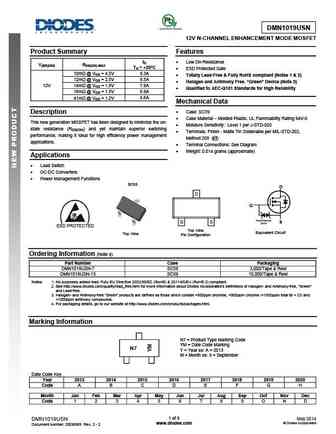
DMN1019USN 12V N-CHANNEL ENHANCEMENT MODE MOSFET Product Summary Features ID Low On-Resistance V(BR)DSS RDS(ON) MAX TA = +25 C ESD Protected Gate 10m @ VGS = 4.5V 9.3A Totally Lead-Free & Fully RoHS compliant (Notes 1 & 2) 12m @ VGS = 2.5V 8.5A Halogen and Antimony Free. Green Device (Note 3) 12V 14m @ VGS = 1.8V 7.9A Qualified to AEC-Q1... See More ⇒
6.2. Size:281K diodes
dmn1019ufde.pdf
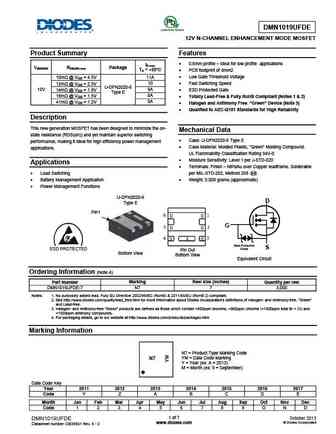
DMN1019UFDE 12V N-CHANNEL ENHANCEMENT MODE MOSFET Product Summary Features 0.6mm profile ideal for low profile applications ID max V(BR)DSS RDS(ON) max Package TA = +25 C PCB footprint of 4mm2 Low Gate Threshold Voltage 10m @ VGS = 4.5V 11A 12m @ VGS = 2.5V 10 Fast Switching Speed U-DFN2020-6 12V 14m @ VGS = 1.8V 9A ESD Protected Gate T... See More ⇒
9.1. Size:147K diodes
dmn100.pdf
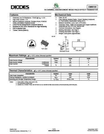
DMN100 N-CHANNEL ENHANCEMENT MODE FIELD EFFECT TRANSISTOR Features Mechanical Data Extremely Low On-Resistance 170m @ VGS = 4.5V Case SC-59 Case Material Molded Plastic, "Green" Molding Compound. High Drain Current 1.1A UL Flammability Classification Rating 94V-0 Ideal for Notebook Computer, Portable Phone, PCMCIA Moisture Sensitivity Level 1 per J-... See More ⇒
9.2. Size:259K diodes
dmn10h099sfg.pdf
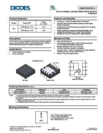
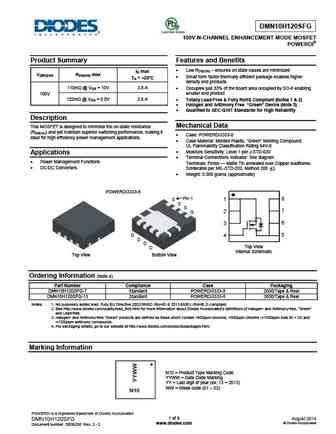
DMN10H099SFG 100V N-CHANNEL ENHANCEMENT MODE MOSFET POWERDI Product Summary Features and Benefits Low RDS(ON) ensures on state losses are minimized ID max V(BR)DSS RDS(ON) max Small form factor thermally efficient package enables higher TA = +25 C density end products 80m @ VGS = 10V 4.2A Occupies just 33% of the board area occupied by SO-8 enabling ... See More ⇒
9.3. Size:398K diodes
dmn1029ufdb.pdf
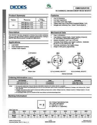
DMN1029UFDB N-CHANNEAL ENHANCEMENT MODE MOSFET Product Summary Features Low On-Resistance ID MAX V(BR)DSS RDS(ON) Max Low Input Capacitance TA = +25 C Low Profile, 0.6mm Max Height 29m @ VGS = 4.5V 5.6A Totally Lead-Free & Fully RoHS Compliant (Notes 1 & 2) 34m @ VGS = 2.5V 5.1A Halogen and Antimony Free. Green Device (Note 3) 12V 4... See More ⇒
9.4. Size:418K diodes
dmn10h120se.pdf
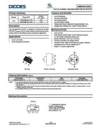
DMN10H120SE 100V N-CHANNEL ENHANCEMENT MODE MOSFET Product Summary Features and Benefits ID max Low On-Resistance V(BR)DSS RDS(ON) max TA = +25 C Low Input Capacitance 110m @ VGS = 10V 3.6A Fast Switching Speed 100V 122m @ VGS = 6.0V 3.4A Low Input/Output Leakage Totally Lead-Free & Fully RoHS Compliant (Notes 1 & 2) Halogen and Antimony Free... See More ⇒
9.5. Size:406K diodes
dmn1045ufr4.pdf
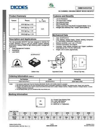
DMN1045UFR4 N-CHANNEL ENHANCEMENT MODE MOSFET Product Summary Features and Benefits Low On-Resistance ID V(BR)DSS RDS(ON) Low Input/Output Leakage TA = +25 C Fast Switching Speed ESD Protected Gate 45m @ VGS = 4.5V Totally Lead-Free & Fully RoHS Compliant (Notes 1 & 2) Halogen and Antimony Free. Green Device (Note 3) 64m @ VGS = 2... See More ⇒
9.6. Size:262K diodes
dmn1025ufdb.pdf
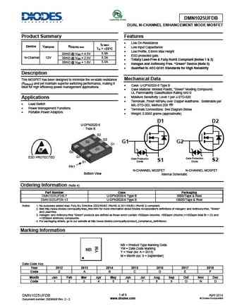
DMN1025UFDB DUAL N-CHANNEL ENHANCEMENT MODE MOSFET Product Summary Features Low On-Resistance ID MAX Device V(BR)DSS RDS(ON) max Low Input Capacitance TA = +25 C Low Profile, 0.6mm Max Height 25m @ VGS = 4.5V 6.9A ESD protected gate. N-Channel 12V 30m @ VGS = 2.5V 6.3A Totally Lead-Free & Fully RoHS Compliant (Notes 1 & 2) 38m @ VGS = 1.8V 5... See More ⇒
9.7. Size:487K diodes
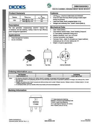
dmn10h100sk3.pdf
DMN10H100SK3 100V N-CHANNEL ENHANCEMENT MODE MOSFET Product Summary Features Low RDS(ON) ensures on state losses are minimized ID BVDSS RDS(ON) max Small form factor thermally efficient package enables higher TC = +25 C 80m @ VGS = 10V 18A density end products 100V 16A 100m @ VGS = 4.5V Totally Lead-Free & Fully RoHS Compliant (Notes 1 & 2) H... See More ⇒
9.8. Size:401K diodes
dmn10h170sfde.pdf
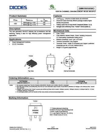
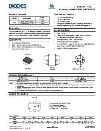
DMN10H170SFDE 100V N-CHANNEL ENHANCEMENT MODE MOSFET Product Summary Features and Benefits 0.6mm Profile Ideal for Low Profile Applications ID max PCB Footprint of 4mm2 V(BR)DSS RDS(ON) max TA = +25 C Low On-Resistance Totally Lead-Free & Fully RoHS Compliant (Notes 1 & 2) 160m @ VGS = 10V 2.9A 100V Halogen and Antimony Free. Green Device ... See More ⇒
9.9. Size:284K diodes
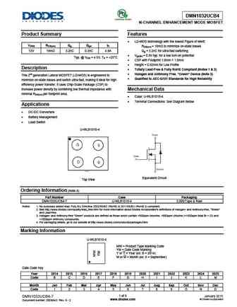
dmn1033ucb4.pdf
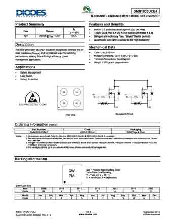
DMN1033UCB4 N-CHANNEL ENHANCEMENT MODE FIELD MOSFET Product Summary Features and Benefits IS Built-in G-S protection diode against ESD 2kV HBM. VSSS RSS(ON) TA = +25 C Totally Lead-Free & Fully RoHS Compliant (Notes 1 & 2) 12V 26m @ VGS = 4.5V 5.5 A Halogen and Antimony Free. Green Device (Note 3) Qualified to AEC-Q101 Standards for High Reliability ... See More ⇒
9.10. Size:508K diodes
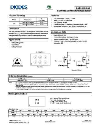
dmn1003uca6.pdf
DMN1003UCA6 N-CHANNEL ENHANCEMENT MODE MOSFET Product Summary Features CSP with Footprint 3.54mm 1.77mm IS Height = 0.21mm for Low Profile BVSSS RSS(ON) Max TA = +25 C ESD Protection of Gate 3.2m @ VGS = 4.5V 23.6A Totally Lead-Free & Fully RoHS Compliant (Notes 1 & 2) 12V 6.3m @ VGS = 2.5V 16.8A Halogen and Antimony Free. Green De... See More ⇒
9.11. Size:303K diodes
dmn10h170sfg.pdf
DMN10H170SFG N-CHANNEL ENHANCEMENT MODE MOSFET POWERDI Product Summary Features ID max 100% Unclamped Inductive Switch (UIS) test in production V(BR)DSS RDS(ON) max TA = +25 C Low RDS(ON) ensures on state losses are minimized 122m @ VGS = 10V 2.9A Small form factor thermally efficient package enables higher 100V 133m @ VGS = 4.5V 2.7A density end ... See More ⇒
9.12. Size:414K diodes
dmn10h170sk3.pdf
DMN10H170SK3 100V N-CHANNEL ENHANCEMENT MODE MOSFET Product Summary Features Low On-Resistance ID V(BR)DSS RDS(on) max Low Input Capacitance TC = +25 C 140m @ VGS = 10V 12A Totally Lead-Free & Fully RoHS Compliant (Notes 1 & 2) 100V 11A 160m @ VGS = 4.5V Halogen and Antimony Free. Green Device (Note 3) Qualified to AEC-Q101 Standards ... See More ⇒
9.13. Size:296K diodes
dmn10h220l.pdf
DMN10H220L 100V N-CHANNEL ENHANCEMENT MODE MOSFET Product Summary Features and Benefits Low On-Resistance ID Low Input Capacitance V(BR)DSS RDS(on) max TA = +25 C Fast Switching Speed Low Input/Output Leakage 220m @ VGS = 10V 1.6A Totally Lead-Free & Fully RoHS Compliant (Notes 1 & 2) 100V 1.3A 250m @ VGS = 4.5V Halogen and Antimony Fre... See More ⇒
9.14. Size:430K diodes
dmn1002uca6.pdf
DMN1002UCA6 N-CHANNEL ENHANCEMENT MODE MOSFET Product Summary Features CSP with Footprint 3.05mm 1.77mm IS BVSSS RSS(ON) Max Height = 0.11mm for Low Profile TA = +25 C ESD Protection of Gate 2.75m @ VGS = 4.5V 24.4A Totally Lead-Free & Fully RoHS Compliant (Notes 1 & 2) 12V 6.1m @ VGS = 2.5V 16.4A Halogen and Antimony Free. Green D... See More ⇒
9.15. Size:236K diodes
dmn10h120sfg.pdf
DMN10H120SFG 100V N-CHANNEL ENHANCEMENT MODE MOSFET POWERDI Product Summary Features and Benefits Low RDS(ON) ensures on state losses are minimized ID max V(BR)DSS RDS(ON) max Small form factor thermally efficient package enables higher TA = +25 C density end products 110m @ VGS = 10V 3.8 A Occupies just 33% of the board area occupied by SO-8 enabling... See More ⇒
9.16. Size:364K diodes
dmn10h220lvt.pdf
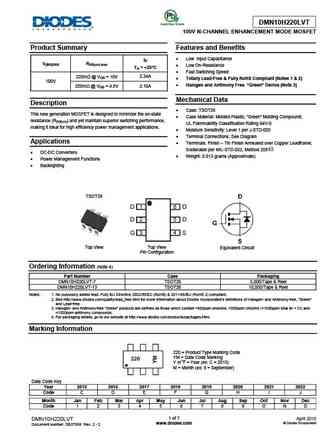
DMN10H220LVT 100V N-CHANNEL ENHANCEMENT MODE MOSFET Product Summary Features and Benefits Low Input Capacitance ID V(BR)DSS RDS(on) max Low On-Resistance TA = +25 C Fast Switching Speed 220m @ VGS = 10V 2.24A Totally Lead-Free & Fully RoHS Compliant (Notes 1 & 2) 100V Halogen and Antimony Free. Green Device (Note 3) 2.10A 250m @ VGS =... See More ⇒
9.17. Size:467K diodes
dmn10h220le.pdf
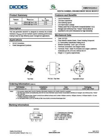
DMN10H220LE 100V N-CHANNEL ENHANCEMENT MODE MOSFET Product Summary Features and Benefits ID Low On-Resistance V(BR)DSS RDS(on) max TA = +25 C Low Input Capacitance 2.3A 220m @ VGS = 10V Fast Switching Speed 100V 250m @ VGS = 4.5V 2.1A Low Input/Output Leakage Totally Lead-Free & Fully RoHS Compliant (Notes 1 & 2) Description Halogen a... See More ⇒
9.18. Size:487K diodes
dmn10h170svt.pdf
DMN10H170SVT N-CHANNEL ENHANCEMENT MODE MOSFET Product Summary Features and Benefits ID max Low Gate Threshold Voltage V(BR)DSS RDS(ON) max TA = +25 C Low Input Capacitance 160m @ VGS = 10V 2.6A Fast Switching Speed 100V 200m @ VGS = 4.5V 2.3A Totally Lead-Free & Fully RoHS Compliant (Notes 1 & 2) Halogen and Antimony Free. Green Device (... See More ⇒
9.19. Size:410K diodes
dmn1006uca6.pdf
DMN1006UCA6 6 N-CHANNEL ENHANCEMENT MODE MOSFET Product Summary Features IS CSP with Footprint 2.70mm 1.81mm BVSSS RSS(ON) MAX TA = +25 C Height = 0.21mm for Low Profile ESD Protection of Gate 5.9m @ VGS = 4.5V 16.6A 12V Totally Lead-Free & Fully RoHS Compliant (Notes 1 & 2) 9.0m @ VGS = 2.5V 12.1A Halogen and Antimony Free. Green De... See More ⇒
9.20. Size:351K diodes
dmn10h099sk3.pdf
DMN10H099SK3 Green 100V N-CHANNEL ENHANCEMENT MODE MOSFET Product Summary Features Low RDS(ON) ensures on state losses are minimized ID V(BR)DSS RDS(on) max Small form factor thermally efficient package enables higher TC = +25 C 80m @ VGS = 10V 17A density end products 100V 99m @ VGS = 6V 15A Lead-Free Finish; RoHS compliant (Note 1 & 2) Haloge... See More ⇒
9.21. Size:286K diodes
dmn1032ucb4.pdf
DMN1032UCB4 N-CHANNEL ENHANCEMENT MODE MOSFET Product Summary Features LD-MOS technology with the lowest Figure of Merit VDSS RDS(on) Qg Qgd ID RDS(on) = 18m to minimize on-state losses 12V 18m 3.2nC 0.3nC 4.8A Qg = 3.2nC for ultra-fast switching Vgs(th) = 0.8V typ. for a low turn-on potential Typ. @ VGS = 4.5V, TA = +25 C CSP with Footprint 1.0mm 1.0mm ... See More ⇒
9.22. Size:89K tysemi
dmn100.pdf
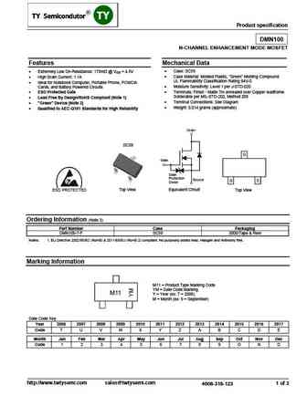
Product specification DMN100 N-CHANNEL ENHANCEMENT MODE MOSFET Features Mechanical Data Extremely Low On-Resistance 170m @ VGS = 4.5V Case SC59 Case Material Molded Plastic, "Green" Molding Compound. High Drain Current 1.1A UL Flammability Classification Rating 94V-0 Ideal for Notebook Computer, Portable Phone, PCMCIA Moisture Sensitivity Level 1 pe... See More ⇒
9.23. Size:265K inchange semiconductor
dmn10h100sk3.pdf

isc N-Channel MOSFET Transistor DMN10H100SK3 FEATURES Drain Current I = 18A@ T =25 D C Drain Source Voltage- V = 100V(Min) DSS Static Drain-Source On-Resistance R = 80m (Max) DS(on) 100% avalanche tested Minimum Lot-to-Lot variations for robust device performance and reliable operation DESCRIPTION Designed for use in switch mode power supplies and general p... See More ⇒
9.24. Size:266K inchange semiconductor
dmn10h099sk3.pdf
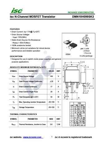
isc N-Channel MOSFET Transistor DMN10H099SK3 FEATURES Drain Current I = 17A@ T =25 D C Drain Source Voltage- V = 100V(Min) DSS Static Drain-Source On-Resistance R = 80m (Max) DS(on) 100% avalanche tested Minimum Lot-to-Lot variations for robust device performance and reliable operation DESCRIPTION Designed for use in switch mode power supplies and general p... See More ⇒
Detailed specifications: DMG9N65CTI, DMGD7N45SSD, DMHC10H170SFJ, DMHC3025LSD, DMHC4035LSD, DMJ7N70SK3, DMN1019UFDE, DMN1019USN, 20N50, DMN1025UFDB, DMN1029UFDB, DMN1032UCB4, DMN1033UCB4, DMN1045UFR4, DMN10H099SFG, DMN10H099SK3, DMN10H100SK3
Keywords - DMN1019UVT MOSFET specs
DMN1019UVT cross reference
DMN1019UVT equivalent finder
DMN1019UVT pdf lookup
DMN1019UVT substitution
DMN1019UVT replacement
Need a MOSFET replacement?
Our guide shows you how to find a perfect substitute by comparing key parameters and specs
