DMN2011UFX Datasheet. Specs and Replacement
Type Designator: DMN2011UFX 📄📄
Type of Transistor: MOSFET
Type of Control Channel: N-Channel
Absolute Maximum Ratings
Pd ⓘ - Maximum Power Dissipation: 2.1 W
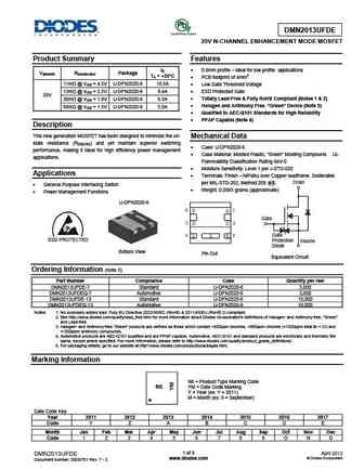
|Vds|ⓘ - Maximum Drain-Source Voltage: 20 V
|Vgs|ⓘ - Maximum Gate-Source Voltage: 12 V
|Id| ⓘ - Maximum Drain Current: 12.2 A
Tj ⓘ - Maximum Junction Temperature: 150 °C
Electrical Characteristics
tr ⓘ - Rise Time: 2.6 nS
Cossⓘ - Output Capacitance: 295 pF
RDSonⓘ - Maximum Drain-Source On-State Resistance: 0.0095 Ohm
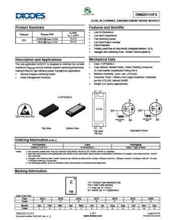
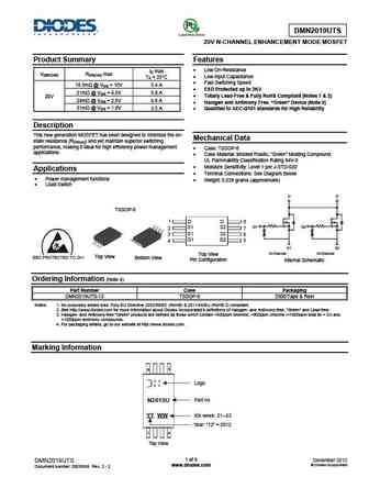
Package: V-DFN2050-4
📄📄 Copy
DMN2011UFX substitution
- MOSFET ⓘ Cross-Reference Search
DMN2011UFX datasheet
dmn2011ufde.pdf
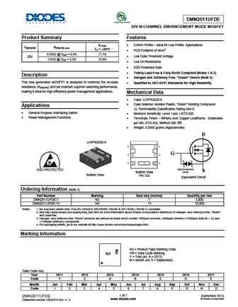
DMN2011UFDE 20V N-CHANNEL ENHANCEMENT MODE MOSFET Product Summary Features ID max 0.6mm Profile Ideal for Low Profile Applications V(BR)DSS RDS(ON) max TA = +25 C PCB Footprint of 4mm2 9.5m @ VGS = 4.5V 11.7A Low Gate Threshold Voltage 20V 11m @ VGS = 2.5V 10.8A Low On-Resistance ESD Protected Gate Totally Lead-Free & Fully RoHS Compl... See More ⇒
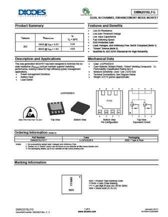
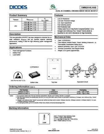
dmn2016lhab.pdf
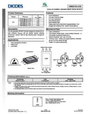
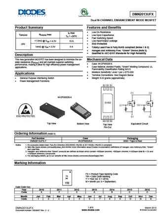
DMN2016LHAB DUAL N-CHANNEL ENHANCEMENT MODE MOSFET Product Summary Features Low On-Resistance ID V(BR)DSS RDS(on)max Low Gate Threshold Voltage TA = +25 C 15.5m @ VGS = 4.5V 7.5A Low Input Capacitance 16.5m @ VGS = 4.0V 7.3A Fast Switching Speed 20V 19m @ VGS = 3.1V 6.9A ESD Protected Gate 20m @ VGS = 2.5V 6.7A Totally Lead-Free & Fully ... See More ⇒
dmn2015ufde.pdf
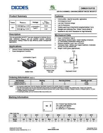
DMN2015UFDE 20V N-CHANNEL ENHANCEMENT MODE MOSFET Product Summary Features 0.6mm profile ideal for low profile applications PCB footprint of 4mm2 ID max V(BR)DSS RDS(ON) max Package TA = +25 C Low Gate Threshold Voltage Low On-Resistance 11.6m @ VGS = 4.5V 10.5A U-DFN2020-6 Totally Lead-Free & Fully RoHS Compliant (Notes 1 & 2) 20V Type E ... See More ⇒
Detailed specifications: DMN10H220LE, DMN10H220LVT, DMN1150UFB, DMN1260UFA, DMN13H750S, DMN15H310SE, DMN2005UFG, DMN2011UFDE, MMIS60R580P, DMN2013UFDE, DMN2013UFX, DMN2014LHAB, DMN2015UFDE, DMN2016LFG, DMN2016LHAB, DMN2019UTS, DMN2020UFCL
Keywords - DMN2011UFX MOSFET specs
DMN2011UFX cross reference
DMN2011UFX equivalent finder
DMN2011UFX pdf lookup
DMN2011UFX substitution
DMN2011UFX replacement
Need a MOSFET replacement? Our guide shows you how to find a perfect substitute by comparing key parameters and specs
