DMN3016LK3 Specs and Replacement
Type Designator: DMN3016LK3
Type of Transistor: MOSFET
Type of Control Channel: N-Channel
Absolute Maximum Ratings
Pd ⓘ - Maximum Power Dissipation: 1.6 W
|Vds|ⓘ - Maximum Drain-Source Voltage: 30 V
|Vgs|ⓘ - Maximum Gate-Source Voltage: 20 V
|Id| ⓘ - Maximum Drain Current: 12.3 A
Tj ⓘ - Maximum Junction Temperature: 150 °C
Electrical Characteristics
tr ⓘ - Rise Time: 16.5 nS
Cossⓘ - Output Capacitance: 119 pF
RDSonⓘ - Maximum Drain-Source On-State Resistance: 0.012 Ohm
Package: TO-252
DMN3016LK3 substitution
- MOSFET ⓘ Cross-Reference Search
DMN3016LK3 datasheet
dmn3016lk3.pdf
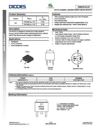
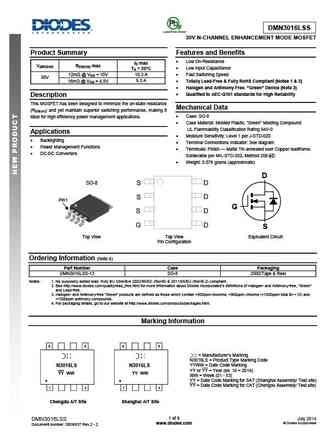
DMN3016LK3 30V N-CHANNEL ENHANCEMENT MODE MOSFET Product Summary Features 100% Unclamped Inductive Switch (UIS) Test in Production ID V(BR)DSS RDS(on) Low On-Resistance TC = +25 C Fast Switching Speed 12m @ VGS = 10V 37.8A Totally Lead-Free & Fully RoHS Compliant (Note 1 & 2) 30V 16m @ VGS = 4.5V 32.8A Halogen and Antimony Free. Green D... See More ⇒
dmn3016lk3.pdf
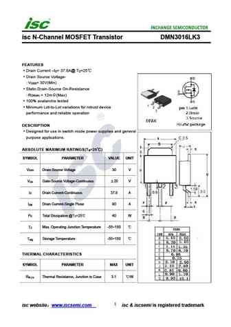
isc N-Channel MOSFET Transistor DMN3016LK3 FEATURES Drain Current I = 37.8A@ T =25 D C Drain Source Voltage- V = 30V(Min) DSS Static Drain-Source On-Resistance R = 12m (Max) DS(on) 100% avalanche tested Minimum Lot-to-Lot variations for robust device performance and reliable operation DESCRIPTION Designed for use in switch mode power supplies and general pu... See More ⇒
dmn3016lps-13.pdf

DMN3016LPS 30V N-CHANNEL ENHANCEMENT MODE MOSFET POWERDI Product Summary Features and Benefits Low On-Resistance ID Low Input Capacitance V(BR)DSS RDS(ON) max TA = +25 C Fast Switching Speed 12m @ VGS = 10V 10.8A ... See More ⇒
dmn3016lps.pdf
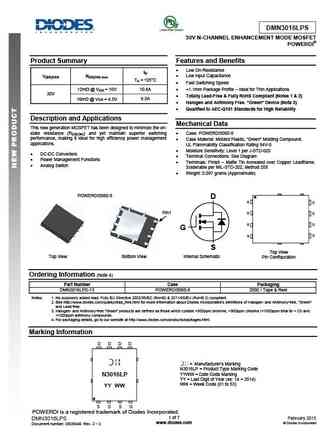
DMN3016LPS 30V N-CHANNEL ENHANCEMENT MODE MOSFET POWERDI Product Summary Features and Benefits Low On-Resistance ID Low Input Capacitance V(BR)DSS RDS(ON) max TA = +25 C Fast Switching Speed 12m @ VGS = 10V 10.8A ... See More ⇒
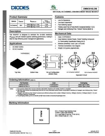
Detailed specifications: DMN2990UFA, DMN2990UFZ, DMN3008SFG, DMN3010LFG, DMN3010LK3, DMN3015LSD, DMN3016LDN, DMN3016LFDE, IRF4905, DMN3016LPS, DMN3016LSS, DMN3018SFG, DMN3018SSD, DMN3018SSS-13, DMN3024SFG, DMN3025LFG, DMN3025LSS
Keywords - DMN3016LK3 MOSFET specs
DMN3016LK3 cross reference
DMN3016LK3 equivalent finder
DMN3016LK3 pdf lookup
DMN3016LK3 substitution
DMN3016LK3 replacement
Can't find your MOSFET? Learn how to find a substitute transistor by analyzing voltage, current and package compatibility
History: PSMN014-60LS | IRFH5020PBF | NVMFD5C650NL | SQ1431EH | RAL035P01
🌐 : EN ES РУ

LIST
Last Update
MOSFET: FTF30P35D | FTF25N35DHVT | FTF15N35D | FTE15C35G | FTP02P15G | FTE02P15G | AKF30N5P0SX | AKF30N10S | AKF20P45D | CM4407
Popular searches
ksa992 transistor | 2n2926 | ksa992 pinout | 2n1308 transistor | p609 | bc327-40 | tip125 | a992 transistor