DMN3070SSN Specs and Replacement
Type Designator: DMN3070SSN
Type of Transistor: MOSFET
Type of Control Channel: N-Channel
Absolute Maximum Ratings
Pd ⓘ - Maximum Power Dissipation: 0.78 W
|Vds|ⓘ - Maximum Drain-Source Voltage: 30 V
|Vgs|ⓘ - Maximum Gate-Source Voltage: 20 V
|Id| ⓘ - Maximum Drain Current: 4.2 A
Tj ⓘ - Maximum Junction Temperature: 150 °C
Electrical Characteristics
tr ⓘ - Rise Time: 20.1 nS
Cossⓘ - Output Capacitance: 97 pF
RDSonⓘ - Maximum Drain-Source On-State Resistance: 0.04 Ohm
Package: SC-59
DMN3070SSN substitution
- MOSFET ⓘ Cross-Reference Search
DMN3070SSN datasheet
dmn3070ssn.pdf
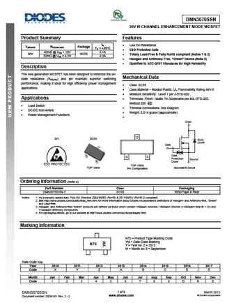
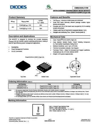
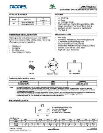
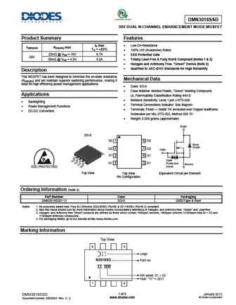
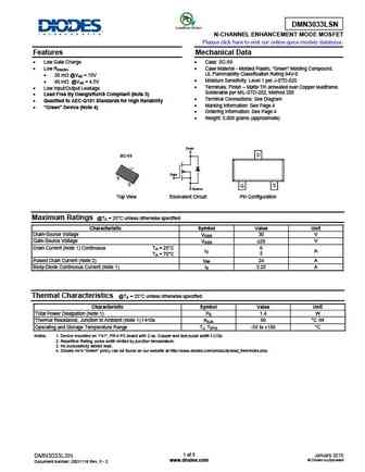
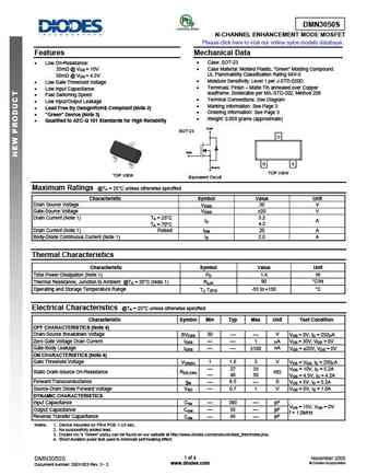
DMN3070SSN 30V N-CHANNEL ENHANCEMENT MODE MOSFET Product Summary Features ID Low On-Resistance V(BR)DSS RDS(ON) MAX Package TA = +25 C ESD Protected Gate 40m @ VGS = 10V 5.1A 30V SC59 Totally Lead-Free & Fully RoHS compliant (Notes 1 & 2) 50m @ VGS = 4.5V 4.3A Halogen and Antimony Free. Green Device (Note 3) Qualified to AEC-Q101 Standard... See More ⇒
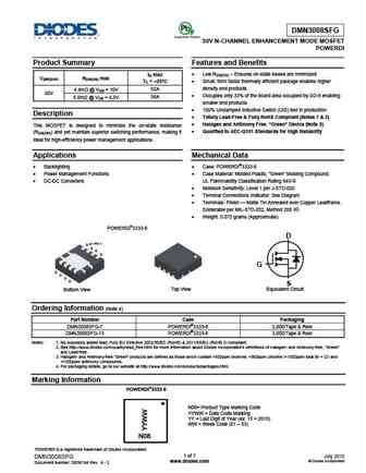
dmn3009lfvw-7.pdf
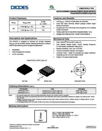
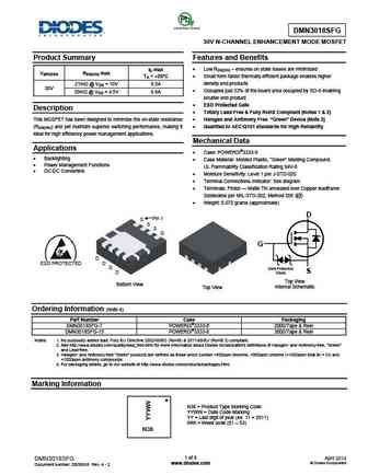
DMN3009LFVW 30V N-CHANNEL ENHANCEMENT MODE MOSFET PowerDI3333-8 (SWP) (Type UX) Product Summary Features and Benefits Low RDS(ON) ensures on state losses are minimized ID max BVDSS RDS(ON) max Small form factor thermally efficient package enables higher TC = +25 C density end products 5.0m @ VGS = 10V 60A Occupies just 33% of the board area occupied b... See More ⇒
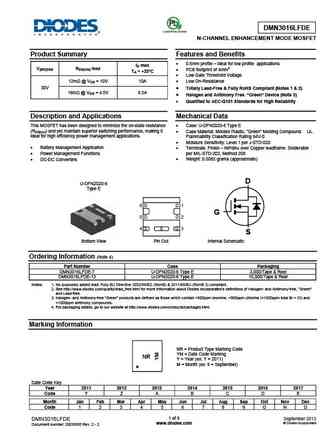
dmn3016lps-13.pdf

DMN3016LPS 30V N-CHANNEL ENHANCEMENT MODE MOSFET POWERDI Product Summary Features and Benefits Low On-Resistance ID Low Input Capacitance V(BR)DSS RDS(ON) max TA = +25 C Fast Switching Speed 12m @ VGS = 10V 10.8A ... See More ⇒
dmn3010lfg-7.pdf
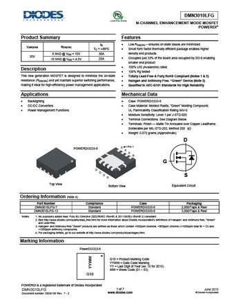
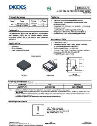
DMN3010LFG N-CHANNEL ENHANCEMENT MODE MOSFET POWERDI Product Summary Features ID Low RDS(ON) ensures on state losses are minimized V(BR)DSS RDS(ON) TC = +25 C Small form factor thermally efficient package enables higher density end products 8.5m @ VGS = 10V 30A 30V Occupies just 33% of the board area occupied by SO-8 enabling 10.5m @ VGS = 4.5V 25A ... See More ⇒
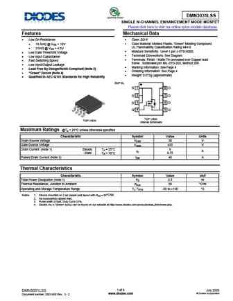
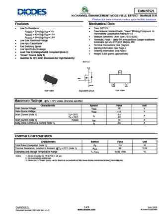
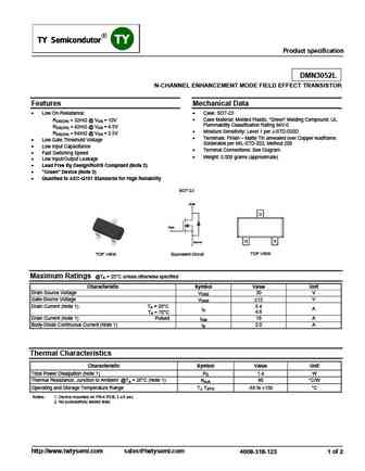
dmn3051l.pdf
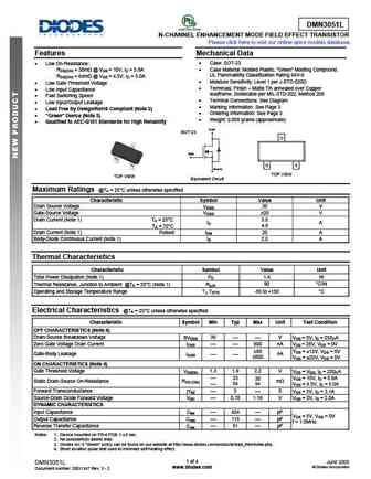
DMN3051L N-CHANNEL ENHANCEMENT MODE FIELD EFFECT TRANSISTOR Please click here to visit our online spice models database. Features Mechanical Data Low On-Resistance Case SOT-23 RDS(ON) ... See More ⇒
dmn3010lfg.pdf

DMN3010LFG N-CHANNEL ENHANCEMENT MODE MOSFET POWERDI Product Summary Features ID Low RDS(ON) ensures on state losses are minimized V(BR)DSS RDS(ON) TC = +25 C Small form factor thermally efficient package enables higher density end products 8.5m @ VGS = 10V 30A 30V Occupies just 33% of the board area occupied by SO-8 enabling 10.5m @ VGS = 4.5V 25A ... See More ⇒
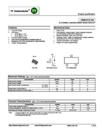
dmn3033lsd.pdf
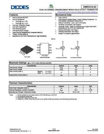
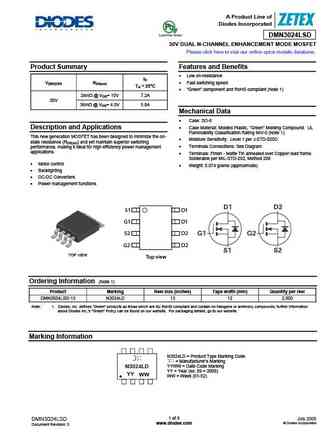
DMN3033LSD DUAL N-CHANNEL ENHANCEMENT MODE FIELD EFFECT TRANSISTOR Please click here to visit our online spice models database. Features Mechanical Data Dual N-Channel MOSFET Case SOP-8L Low On-Resistance Case Material Molded Plastic, Green Molding Compound. UL Flammability Classification Rating 94V-0 22m @ VGS = 10V Moisture Sensitivity Level 1 ... See More ⇒
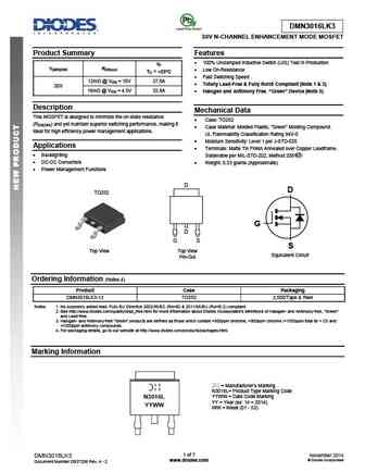
dmn3009sk3.pdf
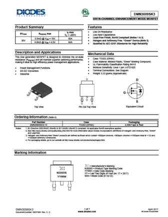
DMN3009SK3 Green 30V N-CHANNEL ENHANCEMENT MODE MOSFET Product Summary Features Low On-Resistance ID max BVDSS RDS(ON) max Low Input Capacitance TC = +25 C Lead-Free Finish; RoHS Compliant (Notes 1 & 2) 5.5m @ VGS = 10V 80A 30V Halogen and Antimony Free. Green Device (Note 3) 9.0m @ VGS = 4.5V 60A Qualified to AEC-Q101 Standards for H... See More ⇒
dmn3005lk3.pdf
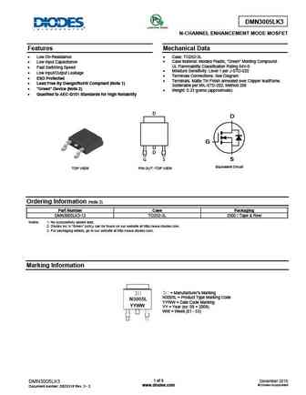
DMN3005LK3 N-CHANNEL ENHANCEMENT MODE MOSFET Features Mechanical Data Low On-Resistance Case TO252-3L Case Material Molded Plastic, Green Molding Compound. Low Input Capacitance UL Flammability Classification Rating 94V-0 Fast Switching Speed Moisture Sensitivity Level 1 per J-STD-020 Low Input/Output Leakage Terminals Connections See... See More ⇒
dmn3042l.pdf
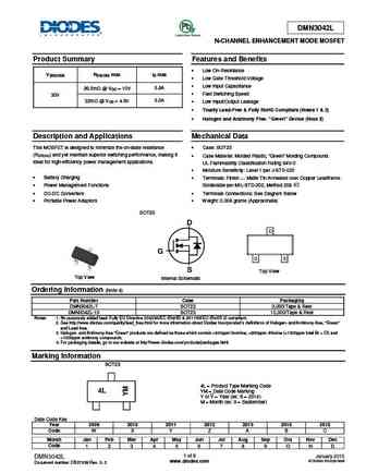
DMN3042L N-CHANNEL ENHANCEMENT MODE MOSFET Product Summary Features and Benefits Low On-Resistance V(BR)DSS RDS(ON) max ID max Low Gate Threshold Voltage Low Input Capacitance 5.8A 26.5m @ VGS = 10V Fast Switching Speed 30V 32m @ VGS = 4.5V 5.0A Low Input/Output Leakage Totally Lead-Free & Fully RoHS Compliant (Notes 1 & 2) Halogen an... See More ⇒
dmn3026lvt.pdf
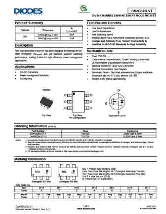
DMN3026LVT 30V N-CHANNEL ENHANCEMENT MODE MOSFET Product Summary Features and Benefits ID Low Input Capacitance V(BR)DSS RDS(on) max TA = +25 C Low On-Resistance Fast Switching Speed 23m @ VGS = 10V 6.6A 30V Totally Lead-Free & Fully RoHS Compliant (Notes 1 & 2) 30m @ VGS = 4.5V 5.8A Halogen and Antimony Free. Green Device (Note 3) Qual... See More ⇒
dmn3032le.pdf
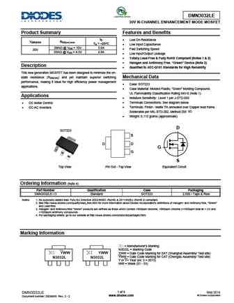
DMN3032LE 30V N-CHANNEL ENHANCEMENT MODE MOSFET Product Summary Features and Benefits ID Low On-Resistance V(BR)DSS RDS(on) max TA = +25 C Low Input Capacitance 29m @ VGS = 10V 5.6A Fast Switching Speed 30V 35m @ VGS = 4.5V 4.8A Low Input/Output Leakage Totally Lead-Free & Fully RoHS Compliant (Notes 1 & 2) Halogen and Antimony Free. Gre... See More ⇒
dmn3035lwn.pdf
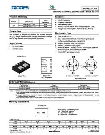
DMN3035LWN 30V DUAL N-CHANNEL ENHANCEMENT MODE MOSFET Product Summary Features Low On-Resistance ID MAX V(BR)DSS RDS(ON) MAX TA = +25 C Low Input Capacitance 35m @ VGS = 10V 5.5A Fast Switching Speed 30V 45m @ VGS = 4.5V 4.9A Totally Lead-Free & Fully RoHS Compliant (Notes 1 & 2) Halogen and Antimony Free. Green Device (Note 3) Descriptio... See More ⇒
dmn3009lfvw.pdf
DMN3009LFVW 30V N-CHANNEL ENHANCEMENT MODE MOSFET PowerDI3333-8 (SWP) (Type UX) Product Summary Features and Benefits Low RDS(ON) ensures on state losses are minimized ID max BVDSS RDS(ON) max Small form factor thermally efficient package enables higher TC = +25 C density end products 5.0m @ VGS = 10V 60A Occupies just 33% of the board area occupied b... See More ⇒
dmn3018sss.pdf
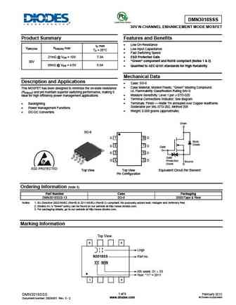
DMN3018SSS 30V N-CHANNEL ENHANCEMENT MODE MOSFET Product Summary Features and Benefits Low On-Resistance ID max V(BR)DSS RDS(ON) max Low Input Capacitance TA = 25 C Fast Switching Speed 21m @ VGS = 10V 7.3A ESD Protected Gate Green component and RoHS compliant (Notes 1 & 2) 30V 35m @ VGS = 4.5V 5.5A Qualified to AEC-Q101 standards for... See More ⇒
dmn3053l.pdf
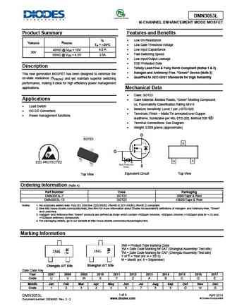
DMN3053L N-CHANNEL ENHANCEMENT MODE MOSFET Product Summary Features and Benefits ID Low On-Resistance V(BR)DSS RDS(ON) TA = +25 C Low Gate Threshold Voltage Low Input Capacitance 45m @ VGS = 10V 4.0 A 30V Fast Switching Speed 50m @ VGS = 4.5V 3.5A Low Input/Output Leakage ESD Protected Gate Description Totally Lead-Free & Fully RoHS Co... See More ⇒
dmn3030lfg.pdf
DMN3030LFG Green N-CHANNEL ENHANCEMENT MODE MOSFET POWERDI Product Summary Features ID Low RDS(ON) ensures on state losses are minimized V(BR)DSS RDS(ON) Package TA = +25 C Small form factor thermally efficient package enables higher 18m @ VGS = 10V POWERDI 8.6A density end products 30V 3333-8 27m @ VGS = 4.5V 5.5A Occupies just 33% of the boa... See More ⇒
dmn3050s.pdf

DMN3050S N-CHANNEL ENHANCEMENT MODE MOSFET Please click here to visit our online spice models database. Features Mechanical Data Low On-Resistance Case SOT-23 35m @ VGS = 10V Case Material Molded Plastic, Green Molding Compound. UL Flammability Classification Rating 94V-0 50m @ VGS = 4.5V Moisture Sensitivity Level 1 per J-STD-020D Low Gate T... See More ⇒
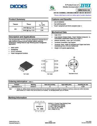
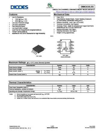
dmn3052lss.pdf
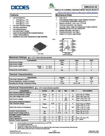
DMN3052LSS SINGLE N-CHANNEL ENHANCEMENT MODE MOSFET Please click here to visit our online spice models database. Features Mechanical Data Low On-Resistance Case SO-8 30m @ VGS = 10V Case Material Molded Plastic, Green Molding Compound. UL Flammability Classification Rating 94V-0 40m @ VGS = 4.5V Moisture Sensitivity Level 1 per J-STD-020 ... See More ⇒
dmn3008sfg.pdf
DMN3008SFG 30V N-CHANNEL ENHANCEMENT MODE MOSFET POWERDI Product Summary Features and Benefits Low RDS(ON) Ensures on-state losses are minimized ID max V(BR)DSS RDS(ON) max TC = +25 C Small, form factor thermally efficient package enables higher density end products 4.4m @ VGS = 10V 62A 30V Occupies only 33% of the board area occupied by SO-8 enabling ... See More ⇒
dmn3016lps.pdf
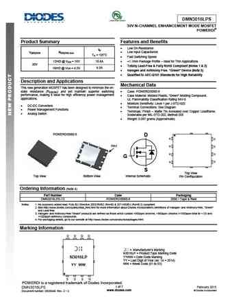
DMN3016LPS 30V N-CHANNEL ENHANCEMENT MODE MOSFET POWERDI Product Summary Features and Benefits Low On-Resistance ID Low Input Capacitance V(BR)DSS RDS(ON) max TA = +25 C Fast Switching Speed 12m @ VGS = 10V 10.8A ... See More ⇒
dmn3031lss.pdf
DMN3031LSS SINGLE N-CHANNEL ENHANCEMENT MODE MOSFET Please click here to visit our online spice models database. Features Mechanical Data Low On-Resistance Case SO-8 18.5m @ VGS = 10V Case Material Molded Plastic, Green Molding Compound. UL Flammability Classification Rating 94V-0 31m @ VGS = 4.5V Moisture Sensitivity Level 1 per J-STD-020D ... See More ⇒
dmn3051ldm.pdf
DMN3051LDM N-CHANNEL ENHANCEMENT MODE MOSFET Please click here to visit our online spice models database. Features Mechanical Data Low On-Resistance Case SOT-26 38 m @ VGS = 10V Case Material Molded Plastic, Green Molding Compound. UL Flammability Classification Rating 94V-0 64 m @ VGS = 4.5V Moisture Sensitivity Level 1 per J-STD-020 Low ... See More ⇒
dmn3024sfg.pdf
DMN3024SFG 30V N-CHANNEL ENHANCEMENT MODE MOSFET POWERDI Product Summary Features and Benefits 100% Unclamped Inductive Switch (UIS) test in production ID max V(BR)DSS RDS(ON) max Low RDS(ON) ensures on state losses are minimized TA = 25 C Small form factor thermally efficient package enables higher 23m @ VGS = 10V 7.5A density end products 30V O... See More ⇒
dmn3067lw.pdf
DMN3067LW N-CHANNEL ENHANCEMENT MODE MOSFET Features and Benefits Product Summary Low On-Resistance ID V(BR)DSS RDS(ON) Low Gate Threshold Voltage TA = +25 C Low Input Capacitance 67m @ VGS = 4.5V 2.6A Fast Switching Speed 30V 70m @ VGS = 4.0V 2.5A Small Surface Mount Package 98m @ VGS = 2.5V 2.2A ESD Protected Gate Totally Lea... See More ⇒
dmn3033lsnq.pdf
DMN3033LSNQ N-CHANNEL ENHANCEMENT MODE MOSFET Product Summary Features Low Gate Charge ID BVDSS RDS(on) max Low RDS(ON) TA = +25 C Low Input/Output Leakage 6A 30m @ VGS = 10V 30V 40m @ VGS = 4.5V 4A Totally Lead-Free & Fully RoHS Compliant (Notes 1 & 2) Halogen and Antimony Free. Green Device (Note 3) Qualified to AEC-Q101 Standa... See More ⇒
dmn3025lss.pdf
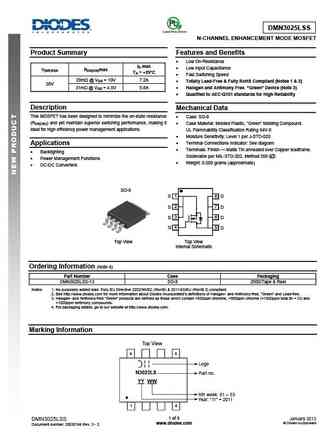
DMN3025LSS N-CHANNEL ENHANCEMENT MODE MOSFET Product Summary Features and Benefits Low On-Resistance ID max Low Input Capacitance V(BR)DSS RDS(ON)max TA = +25 C Fast Switching Speed 20m @ VGS = 10V 7.2A Totally Lead-Free & Fully RoHS Compliant (Notes 1 & 2) 30V 31m @ VGS = 4.5V 5.8A Halogen and Antimony Free. Green Device (Note 3) Qu... See More ⇒
dmn3023l.pdf
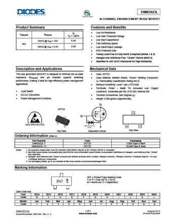
DMN3023L N-CHANNEL ENHANCEMENT MODE MOSFET Product Summary Features and Benefits Low On-Resistance ID V(BR)DSS RDS(ON) TA = +25 C Low Gate Threshold Voltage Low Input Capacitance 6.2A 25m @ VGS = 10V Fast Switching Speed 30V 28m @ VGS = 4.5V 5.8A Low Input/Output Leakage ESD Protected Gate Totally Lead-Free & Fully RoHS Complian... See More ⇒
dmn3010lk3.pdf
DMN3010LK3 Green N-CHANNEL ENHANCEMENT MODE MOSFET Product Summary Features ID Low RDS(ON) ensures on state losses are minimized V(BR)DSS RDS(ON) TC = +25 C Small form factor thermally efficient package enables higher 9.5m @ VGS = 10V 43A density end products 30V 11.5m @ VGS = 4.5V 39A Lead-Free Finish; RoHS Compliant (Notes 1 & 2) Halogen and ... See More ⇒
dmn3018ssd.pdf
DMN3018SSD 30V DUAL N-CHANNEL ENHANCEMENT MODE MOSFET Product Summary Features ID max Low On-Resistance V(BR)DSS RDS(ON) max TA = +25 C 100% UIS (Avalanche) Rated 22m @ VGS = 10V 6.7A ESD Protected Gate 30V 30m @ VGS = 4.5V 5.2A Totally Lead-Free & Fully RoHS Compliant (Notes 1 & 2) Halogen and Antimony Free. Green Device (Note 3) Quali... See More ⇒
dmn3018sfg.pdf
DMN3018SFG 30V N-CHANNEL ENHANCEMENT MODE MOSFET Product Summary Features and Benefits Low RDS(ON) ensures on state losses are minimized ID max V(BR)DSS RDS(ON) max TA = +25 C Small form factor thermally efficient package enables higher density end products 21m @ VGS = 10V 8.5A 30V Occupies just 33% of the board area occupied by SO-8 enabling 35m @ VG... See More ⇒
dmn3016lk3.pdf
DMN3016LK3 30V N-CHANNEL ENHANCEMENT MODE MOSFET Product Summary Features 100% Unclamped Inductive Switch (UIS) Test in Production ID V(BR)DSS RDS(on) Low On-Resistance TC = +25 C Fast Switching Speed 12m @ VGS = 10V 37.8A Totally Lead-Free & Fully RoHS Compliant (Note 1 & 2) 30V 16m @ VGS = 4.5V 32.8A Halogen and Antimony Free. Green D... See More ⇒
dmn3024lk3.pdf
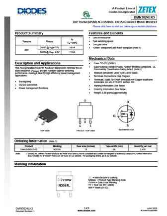
A Product Line of Diodes Incorporated DMN3024LK3 30V TO252 (DPAK) N-CHANNEL ENHANCEMENT MODE MOSFET Please click here to visit our online spice models database. Product Summary Features and Benefits Low on-resistance ID V(BR)DSS RDS(on) Fast switching speed TA = 25 C Low gate drive 24m @ VGS= 10V 14.4A Green component and RoHS compliant (Note 1) 30... See More ⇒
dmn3033ldm.pdf
DMN3033LDM N-CHANNEL ENHANCEMENT MODE MOSFET Please click here to visit our online spice models database. Features Mechanical Data Low Gate Charge Case SOT-26 Low RDS(ON) Case Material - Molded Plastic, Green Molding Compound. UL Flammability Classification Rating 94V-0 33 m @VGS = 10V Moisture Sensitivity Level 1 per J-STD-020D 40 m @VGS ... See More ⇒
dmn3052l.pdf
DMN3052L N-CHANNEL ENHANCEMENT MODE FIELD EFFECT TRANSISTOR Please click here to visit our online spice models database. Features Mechanical Data Low On-Resistance Case SOT-23 RDS(ON) ... See More ⇒
dmn3029lfg.pdf
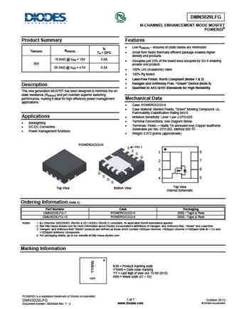
DMN3029LFG Green N-CHANNEL ENHANCEMENT MODE MOSFET POWERDI Product Summary Features Low RDS(ON) ensures on state losses are minimized ID V(BR)DSS RDS(ON) Small form factor thermally efficient package enables higher TA = 25 C density end products 18.6m @ VGS = 10V 8.0A Occupies just 33% of the board area occupied by SO-8 enabling 30V smaller end pr... See More ⇒
dmn3024lsd.pdf
A Product Line of Diodes Incorporated DMN3024LSD 30V DUAL N-CHANNEL ENHANCEMENT MODE MOSFET Please click here to visit our online spice models database. Product Summary Features and Benefits Low on-resistance ID V(BR)DSS RDS(on) Fast switching speed TA = 25 C Green component and RoHS compliant (Note 1) 24m @ VGS= 10V 7.2A 30V 36m @ VGS= 4.5V 5.8A M... See More ⇒
dmn3033lsn.pdf
DMN3033LSN N-CHANNEL ENHANCEMENT MODE MOSFET Please click here to visit our online spice models database. Features Mechanical Data Low Gate Charge Case SC-59 Low RDS(ON) Case Material - Molded Plastic, Green Molding Compound. UL Flammability Classification Rating 94V-0 30 m @VGS = 10V Moisture Sensitivity Level 1 per J-STD-020 40 m @VGS = ... See More ⇒
dmn3020lk3.pdf
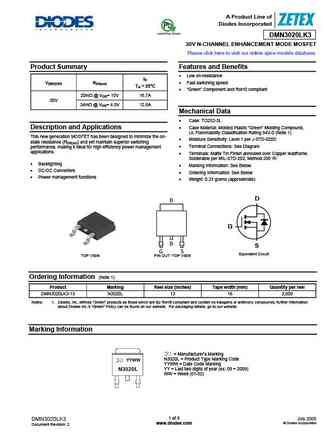
A Product Line of Diodes Incorporated DMN3020LK3 30V N-CHANNEL ENHANCEMENT MODE MOSFET Please click here to visit our online spice models database. Product Summary Features and Benefits Low on-resistance ID V(BR)DSS RDS(on) Fast switching speed TA = 25 C Green Component and RoHS compliant 20m @ VGS= 10V 16.7A 30V 34m @ VGS= 4.5V 12.6A Mechanical Da... See More ⇒
dmn3025lfg.pdf
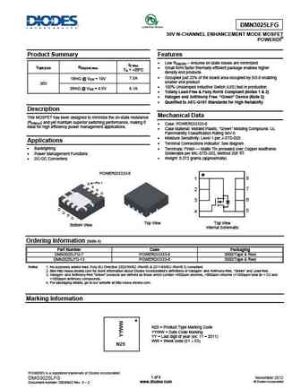
DMN3025LFG 30V N-CHANNEL ENHANCEMENT MODE MOSFET POWERDI Product Summary Features Low RDS(ON) ensures on state losses are minimized ID Max V(BR)DSS RDS(ON) Max Small form factor thermally efficient package enables higher TA = +25 C density end products Occupies just 33% of the board area occupied by SO-8 enabling 18m @ VGS = 10V 7.5A smaller end prod... See More ⇒
dmn3016lss.pdf
DMN3016LSS 30V N-CHANNEL ENHANCEMENT MODE MOSFET Product Summary Features and Benefits Low On-Resistance ID max V(BR)DSS RDS(ON) max Low Input Capacitance TA = 25 C 12m @ VGS = 10V 10.3 A Fast Switching Speed 30V 9.3 A 16m @ VGS = 4.5V Totally Lead-Free & Fully RoHS Compliant (Notes 1 & 2) Halogen and Antimony Free. Green Device (Note 3... See More ⇒
dmn3015lsd.pdf
DMN3015LSD 30V DUAL N-CHANNEL ENHANCEMENT MODE MOSFET Product Summary Features and Benefits Low Input Capacitance ID V(BR)DSS RDS(on) max Low On-Resistance TA = +25 C 15m @ VGS = 10V 8.4A Fast Switching Speed 30V 18m @ VGS = 4.5V 7.7A Totally Lead-Free & Fully RoHS Compliant (Notes 1 & 2) Halogen and Antimony Free. Green Device (Note 3) ... See More ⇒
dmn30h14dly.pdf
DMN30H14DLY N-CHANNEL ENHANCEMENT MODE MOSFET Product Summary Features Low Gate Threshold Voltage ID V(BR)DSS RDS(ON) TA = +25 C Low Input Capacitance Fast Switching Speed 14 @ VGS = 10V 0.21A 300V Totally Lead-Free & Fully RoHS Compliant (Notes 1 & 2) 20 @ VGS = 4.5V 0.17A Halogen and Antimony Free. Green Device (Note 3) Qualified t... See More ⇒
dmn3065lw.pdf
DMN3065LW N-CHANNEL ENHANCEMENT MODE FIELD EFFECT TRANSISTOR Product Summary Features ID max Low On-Resistance V(BR)DSS RDS(ON) Package TA = +25 C Low Gate Threshold Voltage 52m @ VGS = 10V Low Input Capacitance 30V 65m @ VGS = 4.5V SOT323 4A Fast Switching Speed 85m @ VGS = 2.5V Low Input/Output Leakage Totally Lead-Free & Fully RoHS com... See More ⇒
dmn3024lss.pdf
A Product Line of Diodes Incorporated DMN3024LSS 30V N-CHANNEL ENHANCEMENT MODE MOSFET Please click here to visit our online spice models database. Product Summary Features and Benefits Low on-resistance ID V(BR)DSS RDS(on) Fast switching speed TA = 25 C Green component and RoHS compliant (Note 1) 24m @ VGS= 10V 8.5A 30V 36m @ VGS= 4.5V 6.9A Mechan... See More ⇒
dmn3032lfdb.pdf
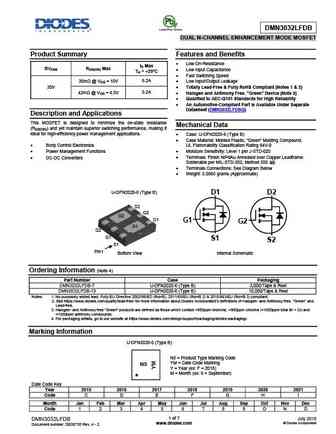
DMN3032LFDB DUAL N-CHANNEL ENHANCEMENT MODE MOSFET Product Summary Features and Benefits Low On-Resistance ID Max BVDSS RDS(ON) Max Low Input Capacitance TA = +25 C Fast Switching Speed 6.2A 30m @ VGS = 10V Low Input/Output Leakage 30V Totally Lead-Free & Fully RoHS Compliant (Notes 1 & 2) 42m @ VGS = 4.5V 5.2A Halogen and Antimony Free... See More ⇒
dmn3016ldn.pdf
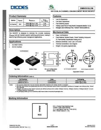
DMN3016LDN 30V DUAL N-CHANNEL ENHANCEMENT MODE MOSFET Product Summary Features Low On-Resistance ID MAX Device V(BR)DSS RDS(ON) max TA = +25 C Low Input Capacitance 20m @ VGS = 10V 7.3A Fast Switching Speed N-Channel 30V 6.7A 24m @ VGS = 4.5V Totally Lead-Free & Fully RoHS Compliant (Notes 1 & 2) Halogen and Antimony Free. Green Dev... See More ⇒
dmn3050s-7.pdf
DMN3050S N-CHANNEL ENHANCEMENT MODE MOSFET Please click here to visit our online spice models database. Features Mechanical Data Low On-Resistance Case SOT-23 35m @ VGS = 10V Case Material Molded Plastic, Green Molding Compound. UL Flammability Classification Rating 94V-0 50m @ VGS = 4.5V Moisture Sensitivity Level 1 per J-STD-020D Low Gate T... See More ⇒
dmn3007lss.pdf
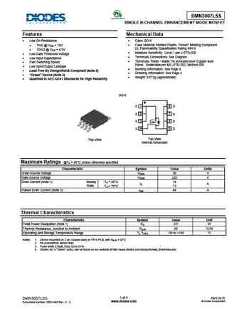
DMN3007LSS SINGLE N-CHANNEL ENHANCEMENT MODE MOSFET Features Mechanical Data Low On-Resistance Case SO-8 7m @ VGS = 10V Case Material Molded Plastic, Green Molding Compound. UL Flammability Classification Rating 94V-0 10m @ VGS = 4.5V Moisture Sensitivity Level 1 per J-STD-020 Low Gate Threshold Voltage Terminals Connections See Di... See More ⇒
dmn30h4d0lfde.pdf
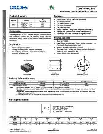
DMN30H4D0LFDE N-CHANNEL ENHANCEMENT MODE MOSFET Product Summary Features ID 0.6mm profile ideal for low profile applications V(BR)DSS RDS(ON) TA = +25 C PCB footprint of 4mm2 4 @ VGS = 10V 0.55A Low Gate Threshold Voltage 300V 4 @ VGS = 4.5V 0.55A Low Input Capacitance 6 @ VGS = 2.7V 0.44A Fast Switching Speed Totally Lead-Free & Fu... See More ⇒
dmn3051l.pdf
Product specification DMN3051L N-CHANNEL ENHANCEMENT MODE MOSFET Product Summary Features and Benefits Low On-Resistance ID V(BR)DSS RDS(ON) Low Gate Threshold Voltage TA = 25 C Low Input Capacitance 38m @ VGS = -10V 5.8A Fast Switching Speed 30V Low Input/Output Leakage 64m @ VGS = -4.5V 4.5A Lead-Free Finish; RoHS compliant (Note 1) ... See More ⇒
dmn3052l.pdf
Product specification DMN3052L N-CHANNEL ENHANCEMENT MODE FIELD EFFECT TRANSISTOR Features Mechanical Data Low On-Resistance Case SOT-23 RDS(ON) ... See More ⇒
dmn3033lsn.pdf
Product specification DMN3033LSN N-CHANNEL ENHANCEMENT MODE MOSFET Features Mechanical Data Low Gate Charge Case SC-59 Low RDS(ON) Case Material - Molded Plastic, Green Molding Compound. UL Flammability Classification Rating 94V-0 30 m @VGS = 10V Moisture Sensitivity Level 1 per J-STD-020 40 m @VGS = 4.5V Terminals Finish Matte ... See More ⇒
dmn3033lsn.pdf
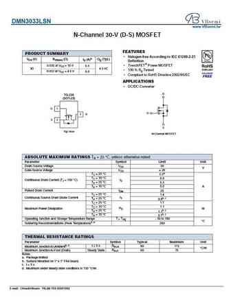
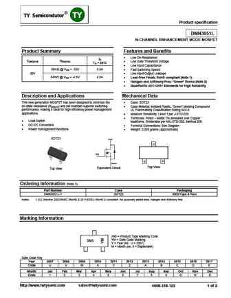
DMN3033LSN www.VBsemi.tw N-Channel 30-V (D-S) MOSFET FEATURES PRODUCT SUMMARY Halogen-free According to IEC 61249-2-21 VDS (V) RDS(on) ( ) ID (A)a Qg (Typ.) Definition 0.030 at VGS = 10 V TrenchFET Power MOSFET 6.5 30 4.5 nC 100 % Rg Tested 0.033 at VGS = 4.5 V 6.0 Compliant to RoHS Directive 2002/95/EC APPLICATIONS DC/DC Converter D TO-236 (SOT-23) ... See More ⇒
dmn3009sk3.pdf

isc N-Channel MOSFET Transistor DMN3009SK3 FEATURES Drain Current I = 80A@ T =25 D C Drain Source Voltage- V = 30V(Min) DSS Static Drain-Source On-Resistance R = 5.5m (Max) DS(on) 100% avalanche tested Minimum Lot-to-Lot variations for robust device performance and reliable operation DESCRIPTION Designed for use in switch mode power supplies and general pur... See More ⇒
dmn3010lk3.pdf

isc N-Channel MOSFET Transistor DMN3010LK3 FEATURES Drain Current I = 43A@ T =25 D C Drain Source Voltage- V = 30V(Min) DSS Static Drain-Source On-Resistance R = 9.5m (Max) DS(on) 100% avalanche tested Minimum Lot-to-Lot variations for robust device performance and reliable operation DESCRIPTION Designed for use in switch mode power supplies and general pur... See More ⇒
dmn3016lk3.pdf

isc N-Channel MOSFET Transistor DMN3016LK3 FEATURES Drain Current I = 37.8A@ T =25 D C Drain Source Voltage- V = 30V(Min) DSS Static Drain-Source On-Resistance R = 12m (Max) DS(on) 100% avalanche tested Minimum Lot-to-Lot variations for robust device performance and reliable operation DESCRIPTION Designed for use in switch mode power supplies and general pu... See More ⇒
dmn3024lk3.pdf
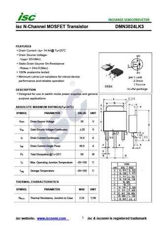
isc N-Channel MOSFET Transistor DMN3024LK3 FEATURES Drain Current I = 14.4A@ T =25 D C Drain Source Voltage- V = 30V(Min) DSS Static Drain-Source On-Resistance R = 24m (Max) DS(on) 100% avalanche tested Minimum Lot-to-Lot variations for robust device performance and reliable operation DESCRIPTION Designed for use in switch mode power supplies and general pu... See More ⇒
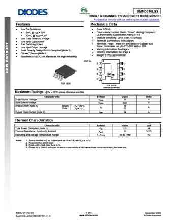
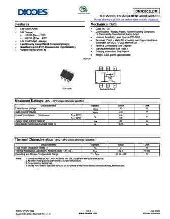
Detailed specifications: DMN3032LE, DMN3033LSNQ, DMN3035LWN, DMN3042L, DMN3050S-7, DMN3053L, DMN3065LW, DMN3067LW, STP80NF70, DMN30H14DLY, DMN30H4D0L, DMN30H4D0LFDE, DMN3135LVT, DMN313DLT, DMN3190LDW, DMN31D5UFZ, DMN32D4SDW
Keywords - DMN3070SSN MOSFET specs
DMN3070SSN cross reference
DMN3070SSN equivalent finder
DMN3070SSN pdf lookup
DMN3070SSN substitution
DMN3070SSN replacement
Can't find your MOSFET? Learn how to find a substitute transistor by analyzing voltage, current and package compatibility
History: SDF10N100JEB
🌐 : EN ES РУ

LIST
Last Update
MOSFET: FTF30P35D | FTF25N35DHVT | FTF15N35D | FTE15C35G | FTP02P15G | FTE02P15G | AKF30N5P0SX | AKF30N10S | AKF20P45D | CM4407
Popular searches
2sc2389 | b331 transistor | 2sa720 | 2sc1345 | 2sd555 | a950 transistor | k2611 | c1740 transistor