DMP1055UFDB Specs and Replacement
Type Designator: DMP1055UFDB
Type of Transistor: MOSFET
Type of Control Channel: P-Channel
Absolute Maximum Ratings
Pd ⓘ
- Maximum Power Dissipation: 1.36 W
|Vds|ⓘ - Maximum Drain-Source Voltage: 12 V
|Vgs|ⓘ - Maximum Gate-Source Voltage: 8 V
|Id| ⓘ - Maximum Drain Current: 3.9 A
Tj ⓘ - Maximum Junction Temperature: 150 °C
Electrical Characteristics
tr ⓘ - Rise Time: 12.8 nS
Cossⓘ -
Output Capacitance: 285 pF
RDSonⓘ - Maximum Drain-Source On-State Resistance: 0.059 Ohm
Package: U-DFN2020-6
- MOSFET ⓘ Cross-Reference Search
DMP1055UFDB datasheet
..1. Size:268K diodes
dmp1055ufdb.pdf 

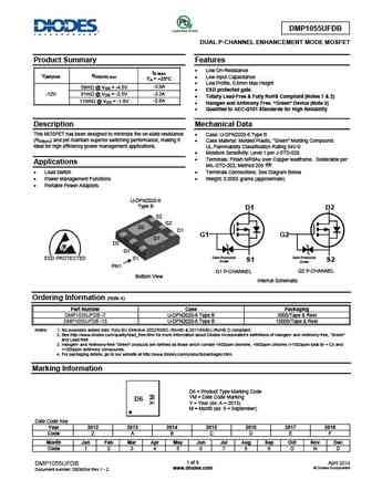
DMP1055UFDB DUAL P-CHANNEL ENHANCEMENT MODE MOSFET Product Summary Features Low On-Resistance ID MAX V(BR)DSS RDS(ON) max Low Input Capacitance TA = +25 C Low Profile, 0.6mm Max Height 59m @ VGS = -4.5V -3.9A ESD protected gate. -12V 81m @ VGS = -2.5V -3.3A Totally Lead-Free & Fully RoHS Compliant (Notes 1 & 2) 115m @ VGS = -1.8V -2.8A ... See More ⇒
6.1. Size:433K diodes
dmp1055usw.pdf 

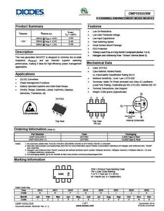
DMP1055USW P-CHANNEL ENHANCEMENT MODE MOSFET Product Summary Features Low On-Resistance ID MAX V(BR)DSS RDS(ON) max TA = +25 C Low Gate Threshold Voltage -3.8A 48m @ VGS = -4.5V Low Input Capacitance -12V -3.4A 59m @ VGS = -2.5V Fast Switching Speed 80m @ VGS = -1.8V -2.9A Small Surface Mount Package ESD Protected Description ... See More ⇒
9.1. Size:479K diodes
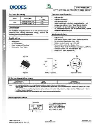
dmp10h400sk3.pdf 

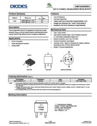
DMP10H400SK3 100V P-CHANNEL ENHANCEMENT MODE MOSFET Product Summary Features ID Low On-Resistance V(BR)DSS RDS(on) max TC = +25 C Low Input Capacitance 240m @ VGS = -10V -9A -100V Totally Lead-Free & Fully RoHS Compliant (Notes 1 & 2) -8A 300m @ VGS = -4.5V Halogen and Antimony Free. Green Device (Note 3) Qualified to AEC-Q101 Standards... See More ⇒
9.2. Size:488K diodes
dmp1005ufdf.pdf 

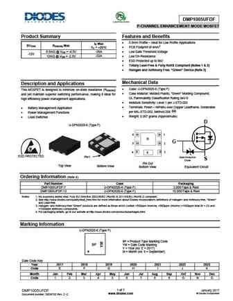
DMP1005UFDF P-CHANNEL ENHANCEMENT MODE MOSFET Product Summary Features and Benefits 0.6mm Profile Ideal for Low Profile Applications ID Max BVDSS RDS(ON) Max PCB Footprint of 4mm2 TC = +25 C 8.5m @ VGS = -4.5V -26A Low Gate Threshold Voltage -12V -22A 12m @ VGS = -2.5V Low On-Resistance ESD Protected up to 8kV Totally Lead-Free & ... See More ⇒
9.3. Size:533K diodes
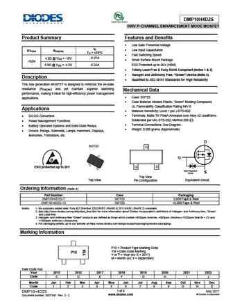
dmp10h4d2s.pdf 

DMP10H4D2S 100V P-CHANNEL ENHANCEMENT MODE MOSFET Product Summary Features and Benefits Low Gate Threshold Voltage ID Low Input Capacitance BVDSS RDS(ON) TA = +25 C Fast Switching Speed 4.2 @ VGS = -10V -0.27A Small Surface Mount Package -100V 5.0 @ VGS = -4.0V -0.24A ESD Protected up to 2KV (HBM) Totally Lead-Free & Fully RoHS Compliant ... See More ⇒
9.4. Size:189K diodes
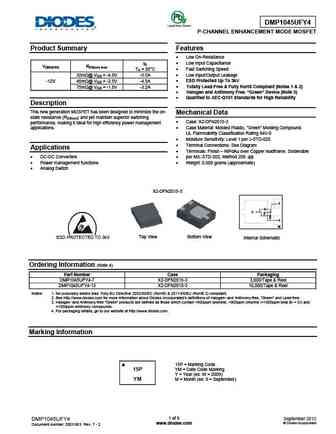
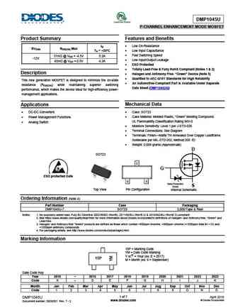
dmp1045ufy4.pdf 

DMP1045UFY4 P-CHANNEL ENHANCEMENT MODE MOSFET Product Summary Features Low On-Resistance ID Low Input Capacitance V(BR)DSS RDS(on) max TA = 25 C Fast Switching Speed 32m @ VGS = -4.5V -5.5A Low Input/Output Leakage -12V 45m @ VGS = -2.5V -4.5A ESD Protected Up To 3kV Totally Lead-Free & Fully RoHS Compliant (Notes 1 & 2) 75m @ VGS = -1.8V -3.2A... See More ⇒
9.5. Size:439K diodes
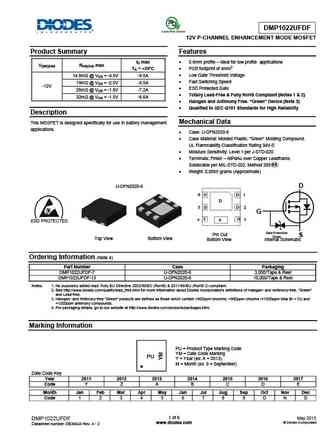
dmp1022ufdf.pdf 

DMP1022UFDF 12V P-CHANNEL ENHANCEMENT MODE MOSFET Product Summary Features ID max 0.6mm profile ideal for low profile applications V(BR)DSS RDS(ON) max TA = +25 C PCB footprint of 4mm2 Low Gate Threshold Voltage 14.8m @ VGS = -4.5V -9.5A Fast Switching Speed 19m @ VGS = -2.5V -8.5A -12V ESD Protected Gate 26m @ VGS = -1.8V -7.2A To... See More ⇒
9.6. Size:361K diodes
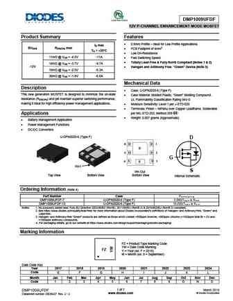
dmp1009ufdf.pdf 

DMP1009UFDF 12V P-CHANNEL ENHANCEMENT MODE MOSFET Product Summary Features 0.6mm Profile Ideal for Low Profile Applications ID max BVDSS RDS(ON) max PCB Footprint of 4mm2 TA = +25 C Low On-Resistance 11m @ VGS = -4.5V -11A Fast Switching Speed Totally Lead-Free & Fully RoHS Compliant (Notes 1 & 2) 14m @ VGS = -3.7V -9.7A -12V Halo... See More ⇒
9.7. Size:232K diodes
dmp1012ucb9.pdf 

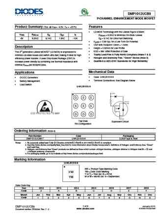
DMP1012UCB9 P-CHANNEL ENHANCEMENT MODE MOSFET Product Summary (Typ. @ VGS = -4.5V, TA = +25 C) Features LD-MOS Technology with the Lowest Figure of Merit VDSS RDS(on) Qg Qgd ID RDS(on) = 8.2m to Minimize On-State Losses -8V 8.2m 8.1nC 1.8nC -10A Qg = 8.1nC for Ultra-Fast Switching Vgs(th) = -0.8V typ. for a Low Turn-On Potential CSP with Footprint 1.5mm 1.... See More ⇒
9.8. Size:152K diodes
dmp1096ucb4.pdf 

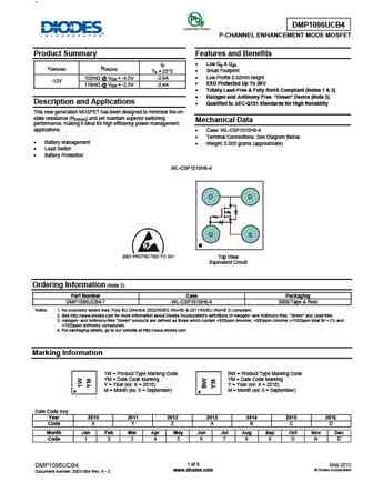
DMP1096UCB4 P-CHANNEL ENHANCEMENT MODE MOSFET Product Summary Features and Benefits Low Qg & Qgd ID V(BR)DSS RDS(ON) Small Footprint TA = 25 C Low Profile 0.62mm height 102m @ VGS = -4.5V -2.6A -12V ESD Protected Up To 3KV 116m @ VGS = -2.5V -2.4A Totally Lead-Free & Fully RoHS Compliant (Notes 1 & 2) Halogen and Antimony Free. Gre... See More ⇒
9.9. Size:396K diodes
dmp1080ucb4.pdf 

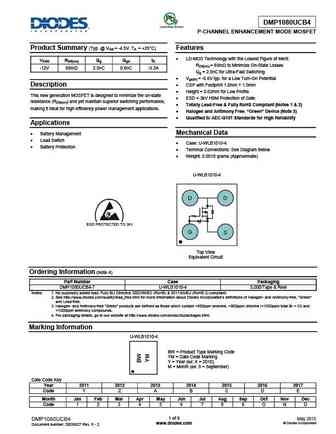
DMP1080UCB4 P-CHANNEL ENHANCEMENT MODE MOSFET Product Summary (Typ. @ VGS = -4.5V, TA = +25 C) Features LD-MOS Technology with the Lowest Figure of Merit VDSS RDS(on) Qg Qgd ID RDS(on) = 65m to Minimize On-State Losses -12V 65m 2.5nC 0.6nC -3.3A Qg = 2.5nC for Ultra-Fast Switching Vgs(th) = -0.6V typ. for a Low Turn-On Potential Description CSP with Footprin... See More ⇒
9.10. Size:457K diodes
dmp1011ucb9.pdf 

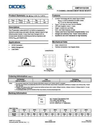
DMP1011UCB9 P-CHANNEL ENHANCEMENT MODE MOSFET Product Summary (Typ. @ VGS = -4.5V, TA = +25 C) Features LD-MOS Technology with the Lowest Figure of Merit VDSS RDS(on) Qg Qgd ID RDS(on) = 8.2m to Minimize On-State Losses -8V 8.2m 8.1nC 1.8nC -10A Qg = 8.1nC for Ultra-Fast Switching Vgs(th) = -0.8V typ. for a Low Turn-On Potential CSP with Footprint 1.5mm 1.5... See More ⇒
9.11. Size:391K diodes
dmp1045u.pdf 

DMP1045U P-CHANNEL ENHANCEMENT MODE MOSFET Product Summary Features and Benefits Low On-Resistance ID BVDSS RDS(ON) Max TA = +25 C Low Input Capacitance Fast Switching Speed 31m @ VGS = -4.5V 5.2A -12V Low Input/Output Leakage 45m @ VGS =-2.5V 4.3A ESD Protected Totally Lead-Free & Fully RoHS Compliant (Notes 1 & 2) Description Ha... See More ⇒
9.13. Size:207K diodes
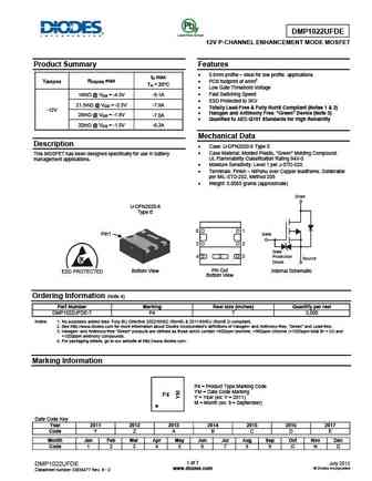
dmp1022ufde.pdf 

DMP1022UFDE 12V P-CHANNEL ENHANCEMENT MODE MOSFET Product Summary Features 0.6mm profile ideal for low profile applications ID max V(BR)DSS RDS(ON) max PCB footprint of 4mm2 TA = 25 C Low Gate Threshold Voltage Fast Switching Speed 16m @ VGS = -4.5V -9.1A ESD Protected to 3KV 21.5m @ VGS = -2.5V -7.9A Totally Lead-Free & Fully RoHS Comp... See More ⇒
9.14. Size:357K diodes
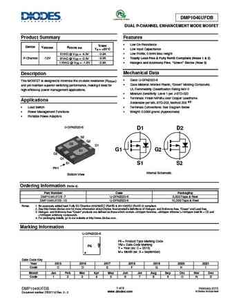
dmp1046ufdb.pdf 

DMP1046UFDB DUAL P-CHANNEL ENHANCEMENT MODE MOSFET Product Summary Features Low On-Resistance ID MAX Device V(BR)DSS RDS(ON) max TA = +25 C Low Input Capacitance Low Profile, 0.6mm Max Height 61m @ VGS = -4.5V -3.8A P-Channel -12V 81m @ VGS = -2.5V -3.3A Totally Lead-Free & Fully RoHS Compliant (Notes 1 & 2) 115m @ VGS = -1.8V -2.8A Halogen and ... See More ⇒
9.15. Size:326K diodes
dmp1018ucb9.pdf 

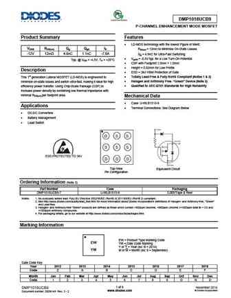
DMP1018UCB9 P-CHANNEL ENHANCEMENT MODE MOSFET Product Summary Features LD-MOS technology with the lowest Figure of Merit VDSS RDS(on) Qg Qgd ID RDS(on) = 12m to Minimize On-State Losses -12V 12m 4.9nC 1.1nC -7.6A Qg = 4.9nC for Ultra-Fast Switching Vgs(th) = -0.8V typ. for a Low Turn-On Potential Typ. @ VGS = -4.5V, TA = +25 C CSP with Footprint 1.5mm 1.5... See More ⇒
9.16. Size:404K diodes
dmp10h400seq.pdf 

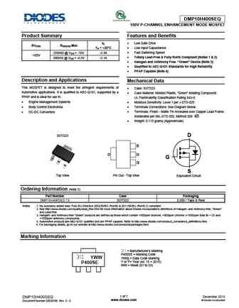
DMP10H400SEQ 100V P-CHANNEL ENHANCEMENT MODE MOSFET Product Summary Features and Benefits ID Low Gate Drive BVDSS RDS(ON) Max TA = +25 C Low Input Capacitance Fast Switching Speed 250m @ VGS = -10V -2.3A -100V Totally Lead-Free & Fully RoHS Compliant (Notes 1 & 2) 300m @ VGS = -4.5V -2.1A Halogen and Antimony Free. Green Device (Note 3) ... See More ⇒
9.17. Size:81K tysemi
dmp1045u.pdf 

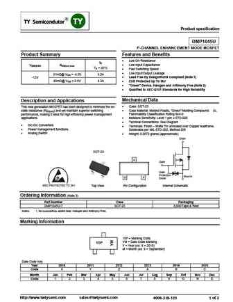
Product specification DMP1045U P-CHANNEL ENHANCEMENT MODE MOSFET Product Summary Features and Benefits Low On-Resistance ID Low Input Capacitance V(BR)DSS RDS(on) max TA = 25 C Fast Switching Speed Low Input/Output Leakage 31m @ VGS = -4.5V 5.2A Lead Free By Design/RoHS Compliant (Note 1) -12V 4.3A 45m @ VGS =-2.5V ESD Protected Up To ... See More ⇒
9.18. Size:266K inchange semiconductor
dmp10h400sk3.pdf 
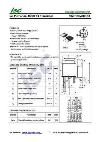
isc P-Channel MOSFET Transistor DMP10H400SK3 FEATURES Drain Current I = -9A@ T =25 D C Drain Source Voltage- V = -100V(Min) DSS Static Drain-Source On-Resistance R = 240m (Max) DS(on) 100% avalanche tested Minimum Lot-to-Lot variations for robust device performance and reliable operation DESCRIPTION Designed for use in switch mode power supplies and general ... See More ⇒
Detailed specifications: DMN7022LFG, DMP1011UCB9, DMP1012UCB9, DMP1018UCB9, DMP1022UFDE, DMP1022UFDF, DMP1045UFY4, DMP1046UFDB, AO3400, DMP1080UCB4, DMP1096UCB4, DMP10H400SK3, DMP1200UFR4, DMP1245UFCL, DMP1555UFA, DMP2002UPS, DMP2006UFG
Keywords - DMP1055UFDB MOSFET specs
DMP1055UFDB cross reference
DMP1055UFDB equivalent finder
DMP1055UFDB pdf lookup
DMP1055UFDB substitution
DMP1055UFDB replacement
Learn how to find the right MOSFET substitute. A guide to cross-reference, check specs and replace MOSFETs in your circuits.
