SFS9624 Datasheet. Specs and Replacement
Type Designator: SFS9624
Type of Transistor: MOSFET
Type of Control Channel: P-Channel
Absolute Maximum Ratings
Pd ⓘ - Maximum Power Dissipation: 28 W
|Vds|ⓘ - Maximum Drain-Source Voltage: 250 V
|Vgs|ⓘ - Maximum Gate-Source Voltage: 30 V
|Id| ⓘ - Maximum Drain Current: 2.4 A
Tj ⓘ - Maximum Junction Temperature: 150 °C
Electrical Characteristics
tr ⓘ - Rise Time: 19 nS
Cossⓘ - Output Capacitance: 65 pF
RDSonⓘ - Maximum Drain-Source On-State Resistance: 2.4 Ohm
Package: TO220F
SFS9624 substitution
- MOSFET ⓘ Cross-Reference Search
SFS9624 datasheet
sfs9624.pdf

Advanced Power MOSFET FEATURES BVDSS = -250 V Avalanche Rugged Technology RDS(on) = 2.4 Rugged Gate Oxide Technology Lower Input Capacitance ID = -2.4 A Improved Gate Charge Extended Safe Operating Area Lower Leakage Current 10 A (Max.) @ VDS = -250V Low RDS(ON) 1.65 (Typ.) 1 2 3 1.Gate 2. Drain 3. Source Absolute Maximum Ratings Symbol Characteristic Va... See More ⇒
sfs9620.pdf
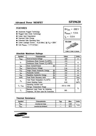
Advanced Power MOSFET FEATURES BVDSS = -200 V Avalanche Rugged Technology RDS(on) = 1.5 Rugged Gate Oxide Technology Lower Input Capacitance ID = -3.0 A Improved Gate Charge Extended Safe Operating Area Lower Leakage Current 10 A (Max.) @ VDS = -200V Low RDS(ON) 1.111 (Typ.) 1 2 3 1.Gate 2. Drain 3. Source Absolute Maximum Ratings Symbol Characteristic V... See More ⇒
sfs9634.pdf
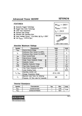
SFS9634 Advanced Power MOSFET FEATURES BVDSS = -250 V Avalanche Rugged Technology RDS(on) = 1.3 Rugged Gate Oxide Technology Lower Input Capacitance ID = -3.4 A Improved Gate Charge Extended Safe Operating Area TO-220F Lower Leakage Current 10 A (Max.) @ VDS = -250V Low RDS(ON) 0.876 (Typ.) 1 2 3 1.Gate 2. Drain 3. Source Absolute Maximum Ratings Symbol ... See More ⇒
sfs9630.pdf
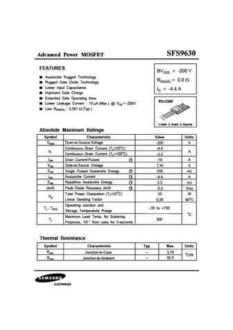
Advanced Power MOSFET FEATURES BVDSS = -200 V Avalanche Rugged Technology RDS(on) = 0.8 Rugged Gate Oxide Technology Lower Input Capacitance ID = -4.4 A Improved Gate Charge Extended Safe Operating Area Lower Leakage Current 10 A (Max.) @ VDS = -200V Low RDS(ON) 0.581 (Typ.) 1 2 3 1.Gate 2. Drain 3. Source Absolute Maximum Ratings Symbol Characteristic V... See More ⇒


Detailed specifications: SFS2955, SFS9510, SFS9520, SFS9530, SFS9540, SFS9610, SFS9614, SFS9620, IRF3205, SFS9630, SFS9634, SFS9640, SFS9644, SFS9Z14, SFS9Z24, SFS9Z34, SFU2955
Keywords - SFS9624 MOSFET specs
SFS9624 cross reference
SFS9624 equivalent finder
SFS9624 pdf lookup
SFS9624 substitution
SFS9624 replacement
Need a MOSFET replacement? Our guide shows you how to find a perfect substitute by comparing key parameters and specs
History: JCS4N80FH
🌐 : EN ES РУ

LIST
Last Update
MOSFET: RM50P30DF | CRTT095N12N | CRSS028N10N | CRST030N10N | CRJQ80N65F | ASDM20N20KQ | ASDM20N100Q | ASDM12N65F | ASDM100R750PKQ | ASDM100R160NKQ
Popular searches
2sc710 | 2sc968 | 2sd217 | bdw93c equivalent | cs7n60f | d613 transistor | fdmc8884 mosfet | k3569 mosfet equivalent