8958 Specs and Replacement
Type Designator: 8958
Type of Transistor: MOSFET
Type of Control Channel: NP-Channel
Absolute Maximum Ratings
Pd ⓘ
- Maximum Power Dissipation: 2 W
|Vds|ⓘ - Maximum Drain-Source Voltage: 30 V
|Vgs|ⓘ - Maximum Gate-Source Voltage: 20 V
|Id| ⓘ - Maximum Drain Current: 6.5 A
Tj ⓘ - Maximum Junction Temperature: 150 °C
Electrical Characteristics
tr ⓘ - Rise Time: 11.2 nS
Cossⓘ -
Output Capacitance: 67 pF
RDSonⓘ - Maximum Drain-Source On-State Resistance: 0.028 Ohm
Package: SOP-8
- MOSFET ⓘ Cross-Reference Search
8958 datasheet
..1. Size:682K sztuofeng
8958.pdf 
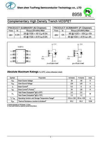
Shen zhen TuoFeng Semiconductor Techonlogy co., LTD Pb 8958 Pb free Complementary High Density Trench MOSFET PRODUCT SUMMARY (N-Channel) PRODUCT SUMMARY (P-Channel) VDSS ID RDS(on) (m-ohm) Max VDSS ID RDS(on) (m-ohm) Max 28 @ VGS = 10 V,ID=6.5A 60 @ VGS = -10V,ID=-5A 6.5A -5A 30V -30V 42 @ VGS = 4.5V,ID=5.0A 90 @ VGS = -4.5V,ID=-4A Absolute Maximum Ratings (T =25oC, unless... See More ⇒
0.1. Size:521K fairchild semi
fds8958a.pdf
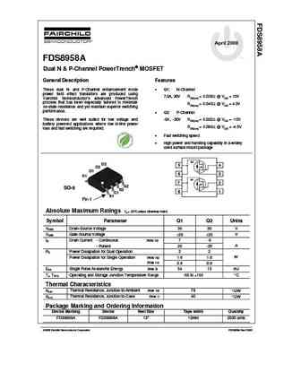
April 2008 tm FDS8958A Dual N & P-Channel PowerTrench MOSFET General Description Features These dual N- and P-Channel enhancement mode Q1 N-Channel power field effect transistors are produced using 7.0A, 30V RDS(on) = 0.028 @ VGS = 10V Fairchild Semiconductor s advanced PowerTrench process that has been especially tailored to minimize RDS(on) = 0.... See More ⇒
0.2. Size:798K fairchild semi
fds8958a f085.pdf
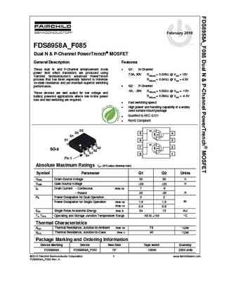
February 2010 tm FDS8958A_F085 Dual N & P-Channel PowerTrench MOSFET General Description Features These dual N- and P-Channel enhancement mode Q1 N-Channel power field effect transistors are produced using 7.0A, 30V RDS(on) = 0.028 @ VGS = 10V Fairchild Semiconductor s advanced PowerTrench process that has been especially tailored to minimize RDS(on... See More ⇒
0.3. Size:222K fairchild semi
nds8958.pdf
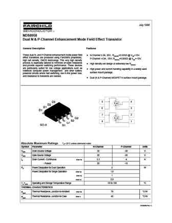
July 1996 NDS8958 Dual N & P-Channel Enhancement Mode Field Effect Transistor General Description Features These dual N- and P-Channel enhancement mode power field N-Channel 5.3A, 30V, RDS(ON)=0.035 @ VGS=10V. effect transistors are produced using Fairchild's proprietary, P-Channel -4.0A, -30V, RDS(ON)=0.065 @ VGS=-10V. high cell density, DMOS technology. This very high density... See More ⇒
0.4. Size:1203K fairchild semi
fds8958b.pdf
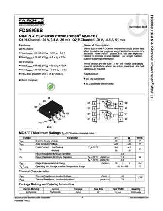
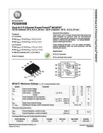
November 2013 FDS8958B Dual N & P-Channel PowerTrench MOSFET Q1-N-Channel 30 V, 6.4 A, 26 m Q2-P-Channel -30 V, -4.5 A, 51 m Features General Description These dual N- and P-Channel enhancement mode power field Q1 N-Channel effect transistors are produced using Fairchild Semiconductor's Max rDS(on) = 26 m at VGS = 10 V, ID = 6.4 A advanced PowerTrench process th at... See More ⇒
0.5. Size:537K onsemi
fds8958a-f085.pdf
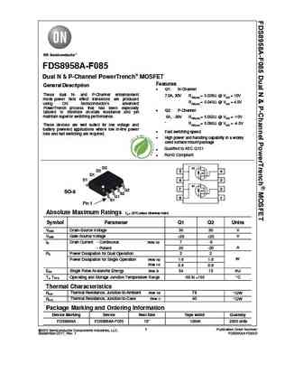
FDS8958A-F085 Dual N & P-Channel PowerTrench MOSFET Features General Description Q1 N-Channel These dual N- and P-Channel enhancement 7.0A, 30V RDS(on) = 0.028 @ VGS = 10V mode power field effect transistors are produced RDS(on) = 0.040 @ VGS = 4.5V using ON Semiconductor s advanced PowerTrench process that has been especially Q2 P-Channel tailored to m... See More ⇒
0.6. Size:635K onsemi
fds8958b.pdf
FDS8958B Dual N & P-Channel PowerTrench MOSFET Q1-N-Channel 30 V, 6.4 A, 26 m Q2-P-Channel -30 V, -4.5 A, 51 m General Description Features These dual N- and P-Channel enhancement mode power field Q1 N-Channel effect transistors are produced using ON Semiconductor's advanced PowerTrench process th at has been especially Max rDS(on) = 26 m at VGS = 10 V, ID = 6.4 A ... See More ⇒
0.7. Size:290K cet
cem8958.pdf
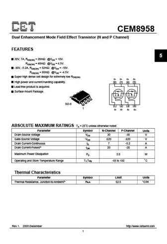
CEM8958 Dual Enhancement Mode Field Effect Transistor (N and P Channel) FEATURES 5 30V, 7A, RDS(ON) = 28m @VGS = 10V. RDS(ON) = 40m @VGS = 4.5V. -30V, -5.2A, RDS(ON) = 52m @VGS = -10V. RDS(ON) = 80m @VGS = -4.5V. Super high dense cell design for extremely low RDS(ON). D1 D1 D2 D2 High power and current handing capability. 8 7 6 5 Lead free product is acquired. Surface... See More ⇒
0.8. Size:421K cet
cem8958a.pdf
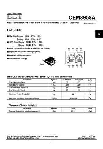
CEM8958A Dual Enhancement Mode Field Effect Transistor (N and P Channel) PRELIMINARY FEATURES 5 30V, 6.8A, RDS(ON) = 28m @VGS = 10V. RDS(ON) = 42m @VGS = 4.5V. -30V, -4.8A, RDS(ON) = 58m @VGS = -10V. RDS(ON) = 85m @VGS = -4.5V. Super high dense cell design for extremely low RDS(ON). D1 D1 D2 D2 8 7 6 5 High power and current handing capability. Lead free product is acq... See More ⇒
0.9. Size:237K analog power
am8958c.pdf
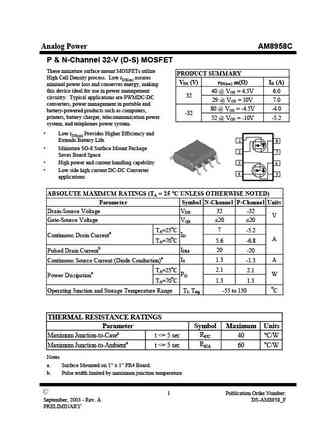
Analog Power AM8958C P & N-Channel 32-V (D-S) MOSFET These miniature surface mount MOSFETs utilize PRODUCT SUMMARY High Cell Density process. Low rDS(on) assures VDS (V) rDS(on) m( )ID (A) minimal power loss and conserves energy, making this device ideal for use in power management 40 @ VGS = 4.5V 6.0 32 circuitry. Typical applications are PWMDC-DC 29 @ V = 10V 7.0 GS conver... See More ⇒
0.10. Size:450K cystek
mtc8958q8.pdf
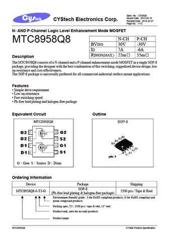
Spec. No. C839Q8 Issued Date 2013.05.10 CYStech Electronics Corp. Revised Date 2014.03.27 Page No. 1/12 N- AND P-Channel Logic Level Enhancement Mode MOSFET N-CH P-CH MTC8958Q8 BVDSS 30V -30V ID 7A -6A RDSON(MAX.) 25m 55m Description The MTC8958Q8 consists of a N-channel and a P-channel enhancement-mode MOSFET in a single SOP-8 package, providing the designer ... See More ⇒
0.11. Size:427K cystek
mtc8958g6.pdf
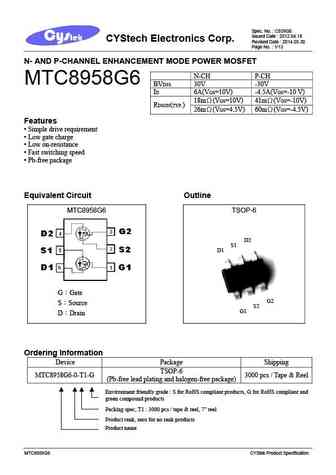
Spec. No. C839G6 Issued Date 2012.04.18 CYStech Electronics Corp. Revised Date 2014.05.30 Page No. 1/13 N- AND P-CHANNEL ENHANCEMENT MODE POWER MOSFET N-CH P-CH MTC8958G6 BVDSS 30V -30V ID 6A(VGS=10V) -4.5A(VGS=-10 V) 18m (VGS=10V) 41m (VGS=-10V) RDSON(TYP.) 26m (VGS=4.5V) 60m (VGS=-4.5V) Features Simple drive requirement Low gate charge Low ... See More ⇒
0.12. Size:78K kexin
kds8958.pdf
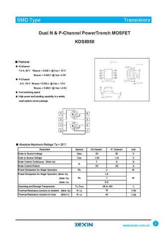
SMD Type IC SMD Type Transistors Dual N & P-Channel PowerTrench MOSFET KDS8958 Features N-Channel 7.0 A, 30 V RDS(ON) = 0.028 @VGS =10V RDS(ON) = 0.040 @VGS =4.5V P-Channel -5 A, -30 V RDS(ON) = 0.052 @VGS =- 10 V RDS(ON) = 0.080 @VGS =-4.5V Fast switching speed High power and handling capability in a widely used surface mount package Absolute Maximum Ratings Ta = 25 Parameter Sy... See More ⇒
0.13. Size:530K ait semi
am8958.pdf
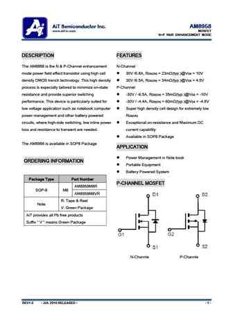
AiT Semiconductor Inc. AM8958 www.ait-ic.com MOSFET N+P PAIR ENHANCEMENT MODE DESCRIPTION FEATURES The AM8958 is the N & P-Channel enhancement N-Channel mode power field effect transistor using high cell 30V /6.8A, R = 23m (typ.)@V = 10V DS(ON) GS density DMOS trench technology. This high density 30V /6.5A, R = 34m (typ.)@V = 4.5V DS(ON) GS process is especially tailor... See More ⇒
0.14. Size:128K chenmko
chm8958jgp.pdf
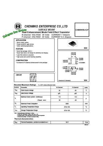
CHENMKO ENTERPRISE CO.,LTD SURFACE MOUNT CHM8958JGP Dual Enhancement Mode Field Effect Transistor N-channel VOLTAGE 30 Volts CURRENT 7 Ampere P-channel VOLTAGE 30 Volts CURRENT 5.2 Ampere APPLICATION * Servo motor control. * Power MOSFET gate drivers. * Other switching applications. SO-8 FEATURE * Small flat package. (SO-8 ) ( ) * Super high dense cell design for extremely low R... See More ⇒
Detailed specifications: 2N6845U, 2N6847U, 2303, 2304, 2305, 4414, 4614, 4800, BS170, 9926, 045Y, 06N03, 10N60A, 10N60AF, 10N60H, 10N80AF, 10N80B
Keywords - 8958 MOSFET specs
8958 cross reference
8958 equivalent finder
8958 pdf lookup
8958 substitution
8958 replacement
Can't find your MOSFET?
Learn how to find a substitute transistor by analyzing voltage, current and package compatibility
