06N03 Specs and Replacement
Type Designator: 06N03
Type of Transistor: MOSFET
Type of Control Channel: N-Channel
Absolute Maximum Ratings
Pd ⓘ
- Maximum Power Dissipation: 150 W
|Vds|ⓘ - Maximum Drain-Source Voltage: 30 V
|Vgs|ⓘ - Maximum Gate-Source Voltage: 20 V
|Id| ⓘ - Maximum Drain Current: 50 A
Tj ⓘ - Maximum Junction Temperature: 175 °C
Electrical Characteristics
tr ⓘ - Rise Time: 19 nS
Cossⓘ -
Output Capacitance: 740 pF
RDSonⓘ - Maximum Drain-Source On-State Resistance: 0.006 Ohm
Package: TO-251
TO-252
- MOSFET ⓘ Cross-Reference Search
06N03 datasheet
..1. Size:117K shenzhen
06n03.pdf 
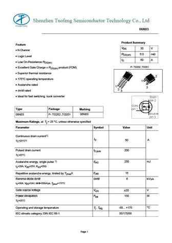
Shenzhen Tuofeng Semiconductor Technology Co., Ltd 06N03 Product Summary Feature VDS 30 V N-Channel RDS(on) 6.0 m Logic Level ID 50 A Low On-Resistance RDS(on) P- TO252 ,TO251 Excellent Gate Charge x RDS(on) product (FOM) Superior thermal resistance 2 175 C operating temperature 1 Avalanche rated 1 3 2 dv/dt rated 3 Ideal for fast switc... See More ⇒
0.1. Size:234K 1
ftd06n03na.pdf
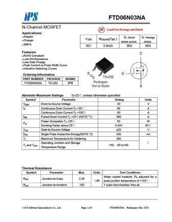
FTD06N03NA N-Channel MOSFET Lead Free Package and Finish Applications Adaptor ID Silicon ID Package VDSS RDS(ON)(Typ.) Charger limited current limited SMPS 30V 3.6m 90A 60A Features RoHS Compliant Low ON Resistance Low Gate Charge Peak Current vs Pulse Width Curve Inductive Switching Curves Ordering Informati... See More ⇒
0.3. Size:274K infineon
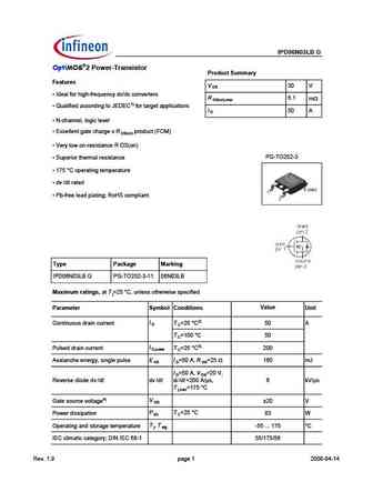
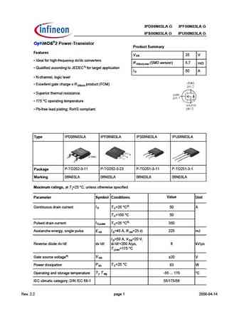
ipb06n03la.pdf
IPB06N03LA G OptiMOS 2 Power-Transistor Product Summary Features V 25 V DS Ideal for high-frequency dc/dc converters R (SMD version) 5.9 m DS(on),max Qualified according to JEDEC1) for target applications I 50 A D N-channel - Logic level Excellent gate charge x R product (FOM) DS(on) Very low on-resistance R DS(on) PG-TO263-3-2 Superior thermal res... See More ⇒
0.4. Size:516K infineon
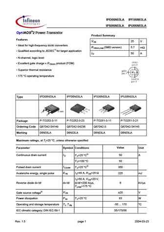
ipu06n03lag.pdf
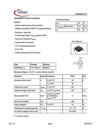
IPD06N03LA G IPF06N03LA G IPS06N03LA G IPU06N03LA G OptiMOS 2 Power-Transistor Product Summary Features V 25 V DS Ideal for high-frequency dc/dc converters R (SMD version) 5.7 m DS(on),max Qualified according to JEDEC1) for target application I 50 A D N-channel, logic level Excellent gate charge x R product (FOM) DS(on) Superior thermal resistance ... See More ⇒
0.6. Size:420K infineon
ipd06n03la ipf06n03la ips06n03la ipu06n03la.pdf
IPD06N03LA IPF06N03LA IPS06N03LA IPU06N03LA OptiMOS 2 Power-Transistor Product Summary Features V 25 V DS Ideal for high-frequency dc/dc converters R (SMD version) 5.7 m DS(on),max Qualified according to JEDEC1) for target application I 50 A D N-channel, logic level Excellent gate charge x R product (FOM) DS(on) Superior thermal resistance 175 C ... See More ⇒
0.7. Size:268K cystek
mta06n03j3.pdf
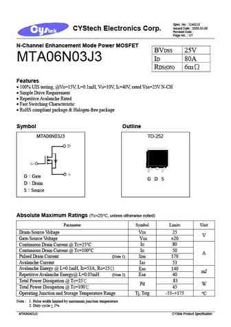
Spec. No. C442J3 Issued Date 2009.03.06 CYStech Electronics Corp. Revised Date Page No. 1/7 N-Channel Enhancement Mode Power MOSFET BVDSS 25V ID 80A MTA06N03J3 RDS(ON) 6m Features 100% UIS testing, @VD=15V, L=0.1mH, VG=10V, IL=40V, rated VDS=25V N-CH Simple Drive Requirement Repetitive Avalanche Rated Fast Switching Characteristic RoHS c... See More ⇒
0.8. Size:292K cystek
mtb06n03j3.pdf
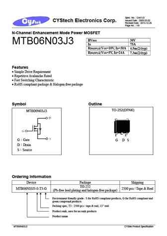
Spec. No. C441J3 Issued Date 2009.03.02 CYStech Electronics Corp. Revised Date 2013.12.26 Page No. 1/9 N-Channel Enhancement Mode Power MOSFET BVDSS 30V MTB06N03J3 ID 75A RDS(ON)@VGS=10V, ID=30A 4.5m (typ) RDS(ON)@VGS=5V, ID=24A 7.3m (typ) Features Simple Drive Requirement Repetitive Avalanche Rated Fast Switching Characteristic RoHS complia... See More ⇒
0.9. Size:281K cystek
mtb06n03e3.pdf
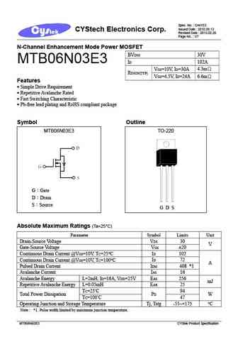
Spec. No. C441E3 Issued Date 2010.08.13 CYStech Electronics Corp. Revised Date 2013.02.26 Page No. 1/7 N-Channel Enhancement Mode Power MOSFET BVDSS 30V MTB06N03E3 ID 102A 4.3m VGS=10V, ID=30A RDSON(TYP) 6.6m VGS=4.5V, ID=24A Features Simple Drive Requirement Repetitive Avalanche Rated Fast Switching Characteristic Pb-free lead plating... See More ⇒
0.10. Size:297K cystek
mta06n03nj3.pdf
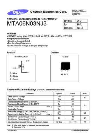
Spec. No. C442J3 Issued Date 2009.03.02 CYStech Electronics Corp. Revised Date Page No. 1/7 N-Channel Enhancement Mode Power MOSFET BVDSS 25V ID 80A MTA06N03NJ3 RDS(ON) 6m Features 100% UIS testing, @VD=15V, L=0.1mH, VG=10V, IL=40V, rated VDS=25V N-CH Simple Drive Requirement Repetitive Avalanche Rated Fast Switching Characteristic RoHS ... See More ⇒
0.11. Size:334K cystek
mtb06n03h8.pdf
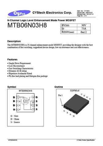
Spec. No. C710H8 Issued Date 2009.05.07 CYStech Electronics Corp. Revised Date 2012.07.31 Page No. 1/11 N-Channel Logic Level Enhancement Mode Power MOSFET BVDSS 30V MTB06N03H8 ID 75A RDSON(max) 6m Description The MTB06N03H8 is a N-channel enhancement-mode MOSFET, providing the designer with the best combination of fast switching, ruggedized device design, low on-... See More ⇒
0.12. Size:328K cystek
mtb06n03v8.pdf
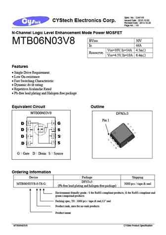
Spec. No. C441V8 Issued Date 2010.10.05 CYStech Electronics Corp. Revised Date 2013.10.30 Page No. 1/9 N-Channel Logic Level Enhancement Mode Power MOSFET BVDSS 30V MTB06N03V8 ID 44A 4.5m VGS=10V, ID=14A RDSON(TYP) 6.4m VGS=4.5V, ID=10A Features Single Drive Requirement Low On-resistance Fast Switching Characteristic Dynamic dv/dt rat... See More ⇒
0.13. Size:309K cystek
mtb06n03q8.pdf
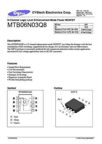
Spec. No. C441Q8 Issued Date 2009.05.07 CYStech Electronics Corp. Revised Date 2012.08.06 Page No. 1/9 N-Channel Logic Level Enhancement Mode Power MOSFET BVDSS 30V MTB06N03Q8 ID 23A RDSON@VGS=10V, ID=18A 4.6m (typ) RDSON@VGS=4.5V, ID=12A 6.5m (typ) Description The MTB06N03Q8 is a N-channel enhancement-mode MOSFET, providing the designer with the best combination ... See More ⇒
0.14. Size:265K cystek
mtb06n03i3.pdf
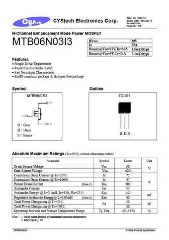
Spec. No. C441I3 Issued Date 2012.02.13 CYStech Electronics Corp. Revised Date Page No. 1/9 N-Channel Enhancement Mode Power MOSFET BVDSS 30V MTB06N03I3 ID 75A RDS(ON)@VGS=10V, ID=30A 4.5m (typ) RDS(ON)@VGS=5V, ID=24A 7.3m (typ) Features Simple Drive Requirement Repetitive Avalanche Rated Fast Switching Characteristic RoHS compliant package ... See More ⇒
0.15. Size:1464K kexin
ndt06n03.pdf
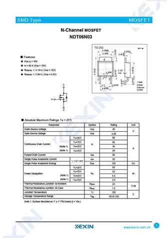
SMD Type MOSFET N-Channel MOSFET NDT06N03 TO-252 Unit mm +0.15 6.50-0.15 +0.1 2.30 -0.1 5.30+0.2 -0.2 +0.8 0.50 -0.7 Features 4 VDS (V) = 30V ID = 60 A (VGS = 10V) RDS(ON) 4.1m (VGS = 10V) 0.127 0.80+0.1 max -0.1 RDS(ON) 5.9m (VGS = 4.5V) 1 Gate + 0.1 D 2 Drain 2.3 0.60- 0.1 +0.15 3 Source 4.60 -0.15 4 Drain G S Absolute Ma... See More ⇒
0.16. Size:992K magnachip
mdp06n033th.pdf
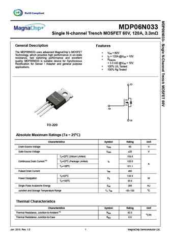
MDP06N033 Single N-channel Trench MOSFET 60V, 120A, 3.3m General Description Features The MDP06N033 uses advanced MagnaChip s MOSFET V = 60V DS Technology, which provides high performance in on-state I = 120A @V = 10V D GS resistance, fast switching performance and excellent R DS(ON) quality. MDP06N033 is suitable device for Synchronous ... See More ⇒
0.17. Size:495K belling
blm06n03-d.pdf
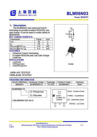
BLM06N03 Power MOSFET 1 Description Step-Down Converter The BLM06N03 uses advanced trench , technology to provide excellent RDS(ON), low gate charge. It can be used in a wide variety of applications. KEY CHARACTERISTICS Parameter Value Unit V 30 V DS I 70 A D R .Typ 6.0 m DS(ON)@10V R .Typ 9.5 m DS(ON)@4.5V FEATURES Advanced Trench Technology ... See More ⇒
0.18. Size:882K way-on
wm06n03ge.pdf

WM06N03GE N-Channel Enhancement MOSFET Features Way-on Small Signal MOSFETs V = 60V, I = 0.34A DS D R ... See More ⇒
0.19. Size:889K way-on
wm06n03le.pdf
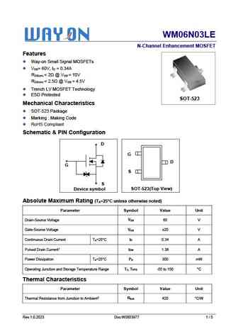
WM06N03LE N-Channel Enhancement MOSFET Features Way-on Small Signal MOSFETs V = 60V, I = 0.34A DS D R ... See More ⇒
0.20. Size:824K way-on
wm06n03m.pdf
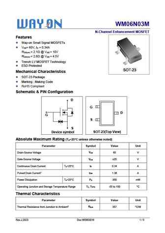
WM06N03M N-Channel Enhancement MOSFET Features Way-on Small Signal MOSFETs V = 60V, I = 0.34A DS D R ... See More ⇒
0.21. Size:462K way-on
wm06n03fb.pdf
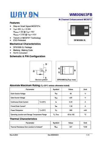
WM06N03FB N-Channel Enhancement MOSFET Features Way-on Small Signal MOSFETs G V = 60V, I = 0.34A DS D D R ... See More ⇒
0.22. Size:809K way-on
wm06n03fe.pdf
WM06N03FE N-Channel Enhancement MOSFET Features Way-on Small Signal MOSFETs V = 60V, I = 0.34A G DS D R ... See More ⇒
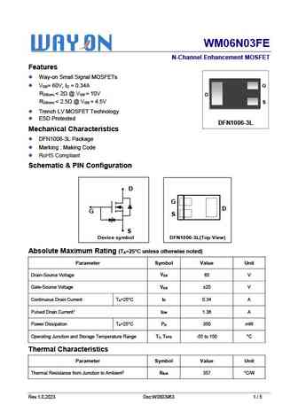
0.23. Size:896K way-on
wm06n03he.pdf
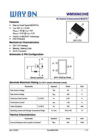
WM06N03HE N-Channel Enhancement MOSFET Features D Way-on Small Signal MOSFETs V = 60V, I = 0.34A DS D R ... See More ⇒
0.24. Size:576K convert
ctd06n030.pdf
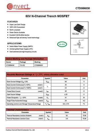
nvert CTD06N030 Suzhou Convert Semiconductor Co ., Ltd. 60V N-Channel Trench MOSFET FEATURES Super Low Gate Charge 100% EAS Guaranteed RoHS compliant Green Device Available Excellent CdV/dt effect decline Advanced high cell density Trench technology APPLICATIONS Switch Mode Power Supply (SMPS) Uninterruptible Power Supply (UPS) Hard switched and... See More ⇒
0.25. Size:753K cn vbsemi
vbze06n03.pdf
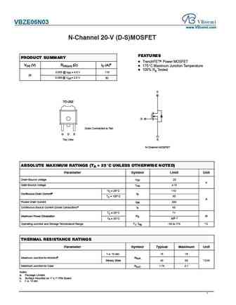
VBZE06N03 www.VBsemi.com N-Channel 20-V (D-S)MOSFET FEATURES PRODUCT SUMMARY D TrenchFETr Power MOSFET VDS (V) RDS(on) (W) ID (A)a D 175_C Maximum Junction Temperature D 100% Rg Tested 0.005 @ VGS = 4.5 V 110 20 20 0.008 @ VGS = 2.5 V 90 D TO-252 G Drain Connected to Tab G D S Top View S N-Channel MOSFET ABSOLUTE MAXIMUM RATINGS (TA = 25_C UNLESS OTHERWISE NOTED) Paramete... See More ⇒
0.26. Size:1062K cn vgsemi
vse006n03msc-g.pdf
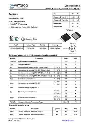
VSE006N03MSC-G 30V/36A N-Channel Advanced Power MOSFET V DS 30 V Features R DS(on),TYP@ VGS=10 V 4.2 m Enhancement mode R DS(on),TYP@ VGS=4.5 V 7.3 m Very low on-resistance I D(Silicon Limited) 48 A VitoMOS Technology I D(Package Limited) 36 A 100% Avalanche Tested,100% Rg Tested PDFN3333 Part ID Package Type Marking Packing VSE006N03MSC-G PDFN3333 006N... See More ⇒
0.27. Size:289K inchange semiconductor
mdp06n033th.pdf
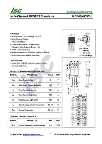
isc N-Channel MOSFET Transistor MDP06N033TH FEATURES Drain Current I = 159.8A@ T =25 D C Drain Source Voltage V = 60V(Min) DSS Static Drain-Source On-Resistance R = 3.3m (Max) @V = 10V DS(on) GS 100% avalanche tested Minimum Lot-to-Lot variations for robust device performance and reliable operation DESCRIPTION motor drive, DC-DC converter, power switch and s... See More ⇒
Detailed specifications: 2304, 2305, 4414, 4614, 4800, 8958, 9926, 045Y, IRF1407, 10N60A, 10N60AF, 10N60H, 10N80AF, 10N80B, 10N90A, 11N10, 11N10G
Keywords - 06N03 MOSFET specs
06N03 cross reference
06N03 equivalent finder
06N03 pdf lookup
06N03 substitution
06N03 replacement
Need a MOSFET replacement?
Our guide shows you how to find a perfect substitute by comparing key parameters and specs