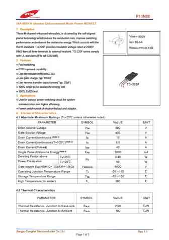
10N80B Specs and Replacement
Type Designator: 10N80B
Type of Transistor: MOSFET
Type of Control Channel: N-Channel
Absolute Maximum Ratings
Pd ⓘ - Maximum Power Dissipation: 240 W
|Vds|ⓘ - Maximum Drain-Source Voltage: 800 V
|Vgs|ⓘ - Maximum Gate-Source Voltage: 30 V
|Id| ⓘ - Maximum Drain Current: 10 A
Tj ⓘ - Maximum Junction Temperature: 150 °C
Electrical Characteristics
tr ⓘ - Rise Time: 130 nS
Cossⓘ - Output Capacitance: 180 pF
RDSonⓘ - Maximum Drain-Source On-State Resistance: 1.1 Ohm
Package: TO-3PB
10N80B substitution
- MOSFET ⓘ Cross-Reference Search
10N80B datasheet
10n80af 10n80b.pdf
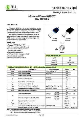
RoHS 10N80 Series RoHS SEMICONDUCTOR Nell High Power Products N-Channel Power MOSFET 10A, 800Volts DESCRIPTION D The Nell 10N80 is a three-terminal silicon device with current conduction capability of 10A, fast switching speed, low on-state resistance, breakdown voltage rating of 800V, and max. threshold voltage of 5 volts. They are designed for use in applications such as G ... See More ⇒
g10n80bf.pdf
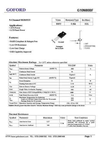
GOFORD G10N80BF N-Channel MOSFET VDSS RDS(on)(Typ) ID (Max) 800V 0.8 10A Applications ATX Power LCD Panel Power Features G RoHS Compliant & Halogen Free DS TO-220F Low ON Resistance Packages Not to Scale Low Gate Charge ESD Capability Improved Absolute Maximum Ratings Tc= 25 unless otherwise specified Symbol Parameter TO-220F Units VDSS Dra... See More ⇒
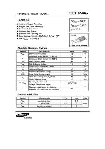
ssh10n80a.pdf
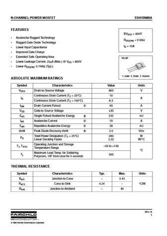
N-CHANNEL POWER MOSFET SSH10N80A FEATURES BVDSS = 800V Avalanche Rugged Technology RDS(ON) = 0.95 Rugged Gate Oxide Technology ID = 10A Lower Input Capacitance Improved Gate Charge Extended Safe Operating Area TO-3P Lower Leakage Current 25 A (Max.) @ VDS = 800V Lower RDS(ON) 0.746 (Typ.) 1 2 3 1. Gate 2. Drain 3. Source ABSOLUTE MAXIMUM RAT... See More ⇒
stf10n80k5.pdf
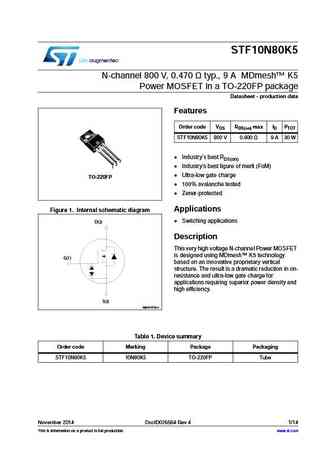
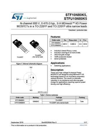
STF10N80K5 N-channel 800 V, 0.470 typ., 9 A MDmesh K5 Power MOSFET in a TO-220FP package Datasheet - production data Features Order code VDS RDS(on) max ID PTOT STF10N80K5 800 V 0.600 9 A 30 W Industry s best RDS(on) 3 2 Industry s best figure of merit (FoM) 1 Ultra-low gate charge TO-220FP 100% avalanche tested Zener-protected Applications F... See More ⇒
stp10n80k5.pdf
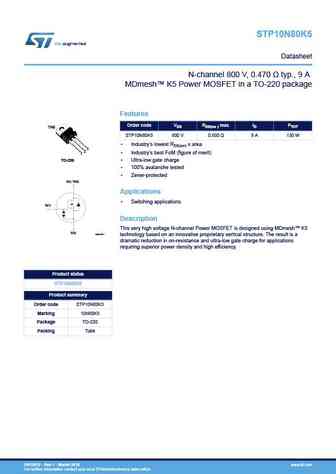
STP10N80K5 Datasheet N-channel 800 V, 0.470 typ., 9 A MDmesh K5 Power MOSFET in a TO-220 package Features Order code VDS RDS(on ) max. ID PTOT TAB STP10N80K5 800 V 0.600 9 A 130 W Industry s lowest RDS(on) x area 3 2 Industry s best FoM (figure of merit) 1 TO-220 Ultra-low gate charge 100% avalanche tested Zener-protected D(2, TAB) Applications... See More ⇒
fdbl0210n80.pdf
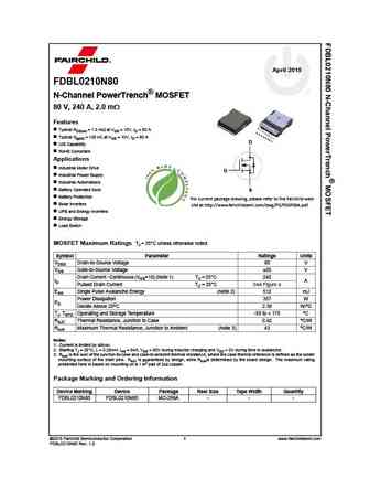
April 2015 FDBL0210N80 N-Channel PowerTrench MOSFET 80 V, 240 A, 2.0 m Features Typical RDS(on) = 1.5 m at VGS = 10V, ID = 80 A Typical Qg(tot) = 130 nC at VGS = 10V, ID = 80 A D UIS Capability RoHS Compliant Applications Industrial Motor Drive G Industrial Power Supply Industrial Automations Battery Operated tools S Battery Protection For current package d... See More ⇒
fqa10n80c.pdf
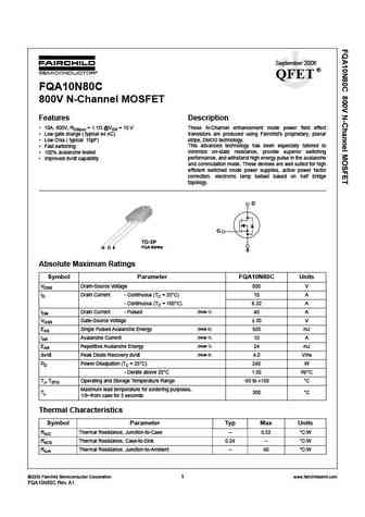
September 2006 QFET FQA10N80C 800V N-Channel MOSFET Features Description 10A, 800V, RDS(on) = 1.1 @VGS = 10 V These N-Channel enhancement mode power field effect Low gate charge ( typical 44 nC) transistors are produced using Fairchild s proprietary, planar stripe, DMOS technology. Low Crss ( typical 15pF) This advanced technology has been especially tailored to ... See More ⇒
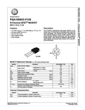
fqa10n80c f109.pdf
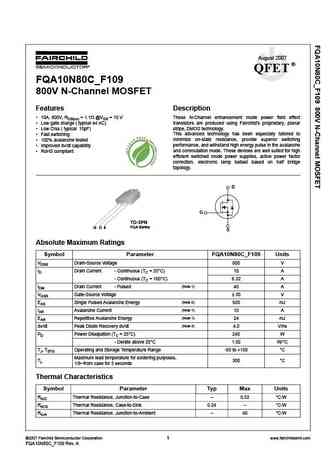
August 2007 QFET FQA10N80C_F109 800V N-Channel MOSFET Features Description 10A, 800V, RDS(on) = 1.1 @VGS = 10 V These N-Channel enhancement mode power field effect Low gate charge ( typical 44 nC) transistors are produced using Fairchild s proprietary, planar stripe, DMOS technology. Low Crss ( typical 15pF) This advanced technology has been especially tailored to... See More ⇒
fqa10n80.pdf
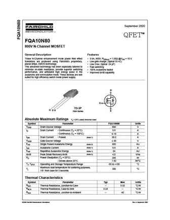
September 2000 TM QFET FQA10N80 800V N-Channel MOSFET General Description Features These N-Channel enhancement mode power field effect 9.8A, 800V, RDS(on) = 1.05 @VGS = 10 V transistors are produced using Fairchild s proprietary, Low gate charge ( typical 55 nC) planar stripe, DMOS technology. Low Crss ( typical 24 pF) This advanced technology has been especially tail... See More ⇒
fqaf10n80.pdf
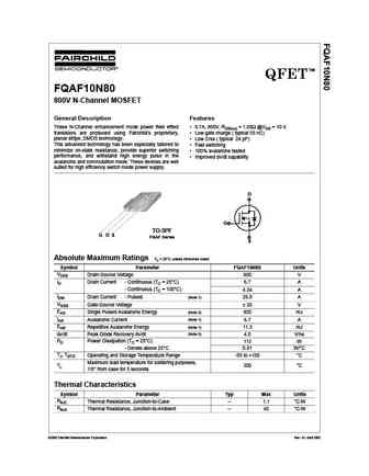
TM QFET FQAF10N80 800V N-Channel MOSFET General Description Features These N-Channel enhancement mode power field effect 6.7A, 800V, RDS(on) = 1.05 @VGS = 10 V transistors are produced using Fairchild s proprietary, Low gate charge ( typical 55 nC) planar stripe, DMOS technology. Low Crss ( typical 24 pF) This advanced technology has been especially tailored to Fa... See More ⇒
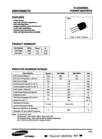
ssh10n70 ssh10n80.pdf
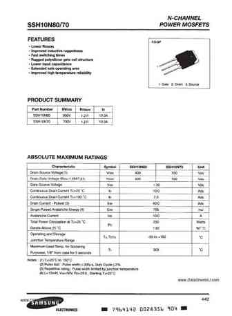
www.DataSheet4U.com www.DataSheet4U.com www.DataSheet4U.com ... See More ⇒
ssh10n80a.pdf
SSH10N80A Advanced Power MOSFET FEATURES BVDSS = 800 V Avalanche Rugged Technology RDS(on) = 0.95 Rugged Gate Oxide Technology Lower Input Capacitance ID = 10 A Improved Gate Charge Extended Safe Operating Area TO-3P Lower Leakage Current 25 A (Max.) @ VDS = 700V Low RDS(ON) 1.552 (Typ.) 1 2 3 1.Gate 2. Drain 3. Source Absolute Maximum Ratings Symbol Cha... See More ⇒
ssf10n80a.pdf
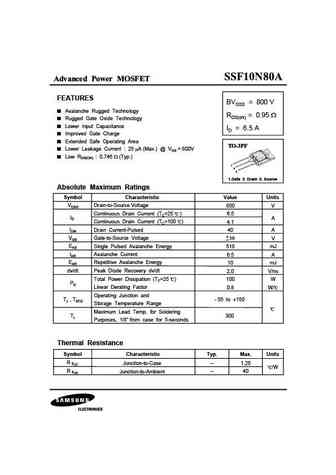
Advanced Power MOSFET FEATURES BVDSS = 800 V Avalanche Rugged Technology RDS(on) = 0.95 Rugged Gate Oxide Technology Lower Input Capacitance ID = 6.5 A Improved Gate Charge Extended Safe Operating Area Lower Leakage Current 25 A (Max.) @ VDS = 800V Low RDS(ON) 0.746 (Typ.) 1 2 3 1.Gate 2. Drain 3. Source Absolute Maximum Ratings Symbol Characteristic Val... See More ⇒
fqa10n80c-f109.pdf
FQA10N80C-F109 N-Channel QFET MOSFET 800 V, 10 A, 1.1 Features Description 10 A, 800 V, RDS(on) = 1.1 (Max.) @ VGS = 10 V, ID = 5 A This N-Channel enhancement mode power MOSFET is pro- duced using ON Semiconductor s proprietary planar stripe and Low Gate Charge (Typ. 44 nC) DMOS technology. This advanced MOSFET technology has Low Crss (Typ. 15 pF) been especiall... See More ⇒
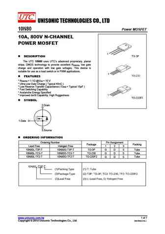
10n80l-t3p-t 10n80g-t3p-t 10n80l-tc3-t 10n80g-tc3-t 10n80l-tf2-t 10n80g-tf2-t.pdf

UNISONIC TECHNOLOGIES CO., LTD 10N80 Power MOSFET 10A, 800V N-CHANNEL POWER MOSFET DESCRIPTION The UTC 10N80 uses UTC s advanced proprietary, planar stripe, DMOS technology to provide excellent RDS(ON), low gate charge and operation with low gate voltages. This device is suitable for use as a load switch or in PWM applications. FEATURES * RDS(ON) ... See More ⇒
10n80.pdf
UNISONIC TECHNOLOGIES CO., LTD 10N80 Power MOSFET 10A, 800V N-CHANNEL POWER MOSFET DESCRIPTION The UTC 10N80 uses UTC s advanced proprietary, planar stripe, DMOS technology to provide excellent RDS(ON), low gate charge and operation with low gate voltages. This device is suitable for use as a load switch or in PWM applications. FEATURES * RDS(ON) ... See More ⇒
fmv10n80e.pdf
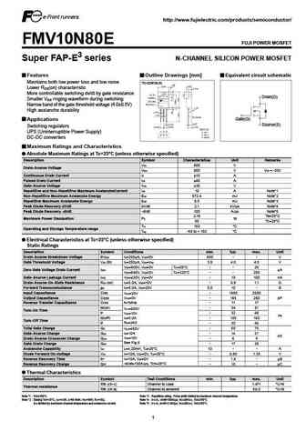
http //www.fujielectric.com/products/semiconductor/ FMV10N80E FUJI POWER MOSFET Super FAP-E3 series N-CHANNEL SILICON POWER MOSFET Features Outline Drawings [mm] Equivalent circuit schematic Maintains both low power loss and low noise TO-220F(SLS) Lower R (on) characteristic DS More controllable switching dv/dt by gate resistance Drain(D) Smaller V ringing waveform during switching G... See More ⇒
tsm10n80ci tsm10n80cz.pdf
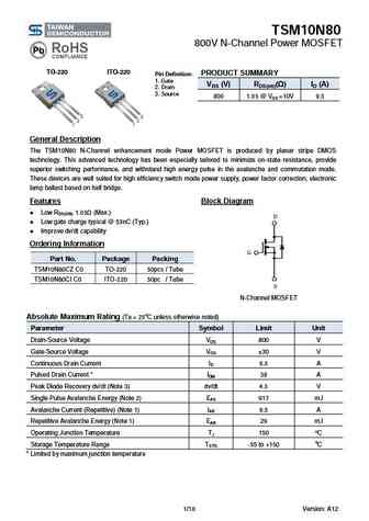
TSM10N80 800V N-Channel Power MOSFET TO-220 ITO-220 PRODUCT SUMMARY Pin Definition 1. Gate VDS (V) RDS(on)( ) ID (A) 2. Drain 3. Source 800 1.05 @ VGS =10V 9.5 General Description The TSM10N80 N-Channel enhancement mode Power MOSFET is produced by planar stripe DMOS technology. This advanced technology has been especially tailored to minimize on-state resistance, pr... See More ⇒
jcs10n80fc jcs10n80gdc.pdf
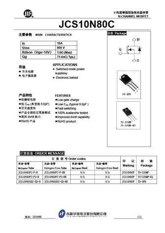
N R N-CHANNEL MOSFET JCS10N80C Package MAIN CHARACTERISTICS 10A ID 800 V VDSS Rdson Vgs=10V 1.0 (Max) 71.6nC( Typ.) Qg APPLICATIONS Switched mode power suppliesy Electronic ballast FEATURES Low gate ch... See More ⇒
jcs10n80f.pdf
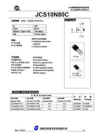
N R N-CHANNEL MOSFET JCS10N80C Package MAIN CHARACTERISTICS 10A ID 800 V VDSS Rdson Vgs=10V 1.0 (Max) 71.6nC( Typ.) Qg APPLICATIONS Switched mode power suppliesy Electronic ballast FEATURES Low gate ch... See More ⇒
brf10n80.pdf
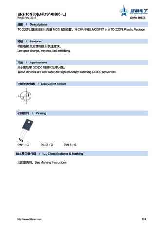
BRF10N80(BRCS10N80FL) Rev.C Feb.-2015 DATA SHEET / Descriptions TO-220FL N MOS N-CHANNEL MOSFET in a TO-220FL Plastic Package. / Features , , Low gate charge, low crss, fast switching. / Applications DC/DC These devices are well suited f... See More ⇒
cs10n80 and.pdf
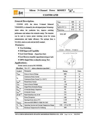
Silicon N-Channel Power MOSFET R CS10N80 AND General Description VDSS 800 V CS10N80 AND, the silicon N-channel Enhanced ID 10 A PD(TC=25 ) 160 W VDMOSFETs, is obtained by the self-aligned planar Technology RDS(ON)Typ 0.72 which reduce the conduction loss, improve switching performance and enhance the avalanche energy. The transistor can be used in various pow... See More ⇒
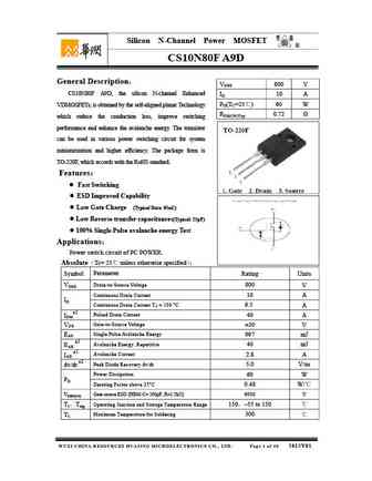
cs10n80f a9d.pdf

Silicon N-Channel Power MOSFET R CS10N80F A9D General Description VDSS 800 V CS10N80F A9D, the silicon N-channel Enhanced ID 10 A PD(TC=25 ) 60 W VDMOSFETs, is obtained by the self-aligned planar Technology RDS(ON)Typ 0.72 which reduce the conduction loss, improve switching performance and enhance the avalanche energy. The transistor can be used in various ... See More ⇒
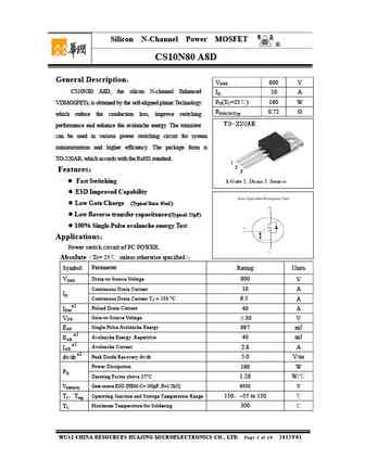
cs10n80 a8d.pdf

Silicon N-Channel Power MOSFET R CS10N80 A8D General Description VDSS 800 V CS10N80 A8D, the silicon N-channel Enhanced ID 10 A PD(TC=25 ) 160 W VDMOSFETs, is obtained by the self-aligned planar Technology RDS(ON)Typ 0.72 which reduce the conduction loss, improve switching performance and enhance the avalanche energy. The transistor can be used in various po... See More ⇒
f10n80.pdf
F10N80 10A 800V N-channel Enhancement Mode Power MOSFET 1 Description These N-channel enhanced vdmosfets, is obtained by the self-aligned V DSS = 800V planar technology which reduce the conduction loss, improve switching I = 10.0A D performance and enhance the avalanche energy. Which accords with the RoHS standard. TO-220F provides insulation voltage rated at 2000V R DS(on) TYP) ... See More ⇒
svf10n80f svf10n80k.pdf
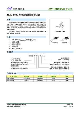
SVF10N80F/K 10A 800V N 2 SVF10N80F/K N MOS F-CellTM VDMOS 1 3 ... See More ⇒
msw10n80.pdf
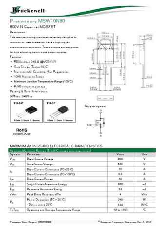
Preliminary MSW10N80 800V N-Channel MOSFET Description This latest technology has been especially designed to minimize on-state resistance, have a high rugged avalanche characteristics. These devices are well suited for high efficiency switch mode power supplies. Features RDS(on) (typ 0.65 )@VGS=10V Gate Charge (Typical 55nC) Improved dv/dt Capability, High Ru... See More ⇒
msf10n80.pdf
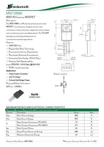
MSF10N80 800V N-Channel MOSFET Description The MSF10N80 is a N-channel enhancement-mode MOSFET , providing the designer with the best combination of fast switching, ruggedized device design, low on-resistance and cost effectiveness. The TO-220F package is universally preferred for all commercial-industrial applications Features 100% EAS Test Rugged Gate Oxide Techn... See More ⇒
ms10n80.pdf
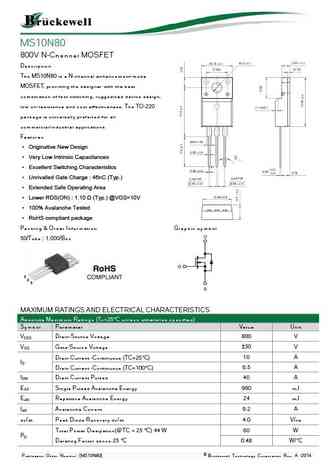
MS10N80 800V N-Channel MOSFET Description The MS10N80 is a N-channel enhancement-mode MOSFET, providing the designer with the best combination of fast switching, ruggedized device design, low on-resistance and cost effectiveness. The TO-220 package is universally preferred for all commercial-industrial applications Features Originative New Design Very Low Intrinsic... See More ⇒
msf10n80a.pdf
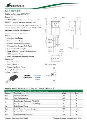
MSF10N80A 800V N-Channel MOSFET Description The MSF10N80A is a N-channel enhancement-mode MOSFET , providing the designer with the best combination of fast switching, ruggedized device design, low on-resistance and cost effectiveness. The TO-220F package is universally preferred for all commercial-industrial applications Features Originative New Design Very Low Int... See More ⇒
bl10n80-p bl10n80-a bl10n80-w bl10n80-f.pdf
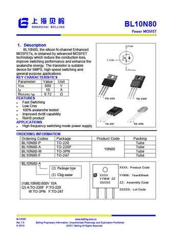
BL10N80 Power MOSFET 1 Description Step-Down Converter BL10N80, the silicon N-channel Enhanced , MOSFETs, is obtained by advanced MOSFET technology which reduce the conduction loss, improve switching performance and enhance the avalanche energy. The transistor is suitable device for SMPS, high speed switching and general purpose applications. KEY CHARACTERISTICS Pa... See More ⇒
fhf10n80a.pdf
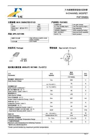
N N-CHANNEL MOSFET FHF10N80A MAIN CHARACTERISTICS FEATURES ID 10A Low gate charge VDSS 800V Crss ( 20pF) Low Crss (typical 20pF ) Rdson-typ @Vgs=10V 0.72 Fast switching Qg-typ 58nC 100% 100% avalanche tested dv/dt Improved dv/d... See More ⇒
jfpc10n80c jffm10n80c.pdf
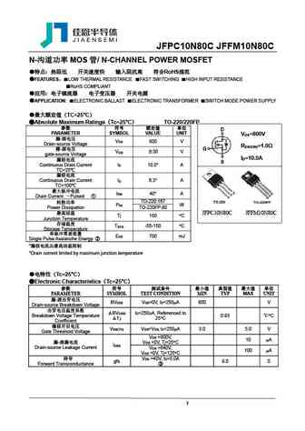
JFPC10N80C JFFM10N80C N- MOS / N-CHANNEL POWER MOSFET RoHS FEATURES LOW THERMAL RESISTANCE FAST SWITCHING HIGH INPUT RESISTANCE RoHS COMPLIANT APPLICATION ELECTRONIC BALLAST ELECTRONIC TRANSFORMER SWITCH MODE POWER ... See More ⇒
kia10n80h.pdf
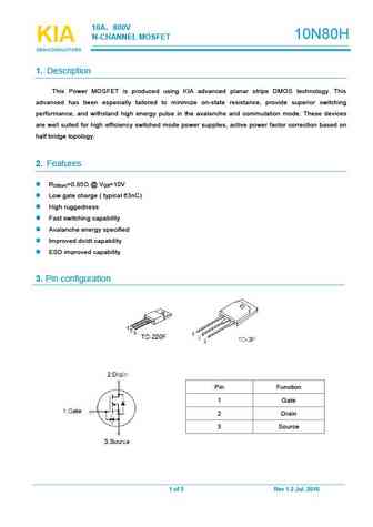
10A 800V 10N80H N-CHANNELMOSFET KIA KIA KIA SEMICONDUCTORS SEMICONDUCTORS SEMICONDUCTORS 1. Description This Power MOSFET is produced using KIA advanced planar stripe DMOS technology. This advanced has been especially tailored to minimize on-state resistance, provide superior switching performance, and withstand high energy pulse in the avalanche and commutation mode. These device... See More ⇒
ptp10n80 pta10n80.pdf

PTP10N80 PTA10N80 800V N-Channel MOSFET General Features BVDSS RDS(ON),typ. ID Proprietary New Planar Technology 800V 1.0 10A RDS(ON),typ.=1.0 @VGS=10V Low Gate Charge Minimize Switching Loss Fast Recovery Body Diode Applications ATX Power G LCD Panel Power D S G D S Ordering Information Part Number Package Brand TO-220 TO-220F ... See More ⇒
swf10n80k2 swn10n80k2 swd10n80k2.pdf
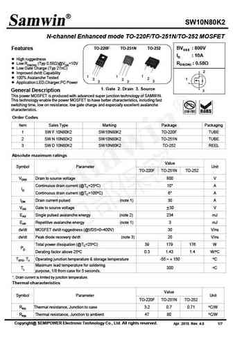
SW10N80K2 N-channel Enhanced mode TO-220F/TO-251N/TO-252 MOSFET TO-220F TO-251N TO-252 BVDSS 800V Features ID 10A High ruggedness RDS(ON) 0.58 Low RDS(ON) (Typ 0.58 )@VGS=10V Low Gate Charge (Typ 27nC) 2 Improved dv/dt Capability 1 1 1 100% Avalanche Tested 2 1 2 2 3 3 3 Application LED,Charger,PC Power 1. Gate 2. Drain ... See More ⇒
swf10n80d.pdf
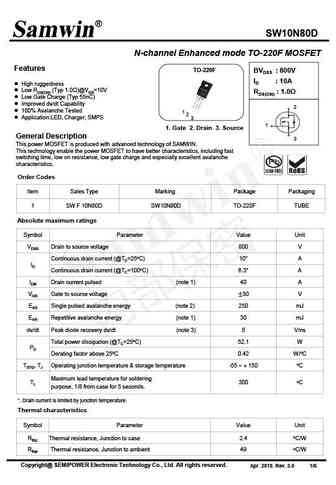
SW10N80D N-channel Enhanced mode TO-220F MOSFET Features TO-220F BVDSS 800V ID 10A High ruggedness Low RDS(ON) (Typ 1.0 )@VGS=10V RDS(ON) 1.0 Low Gate Charge (Typ 55nC) Improved dv/dt Capability 2 100% Avalanche Tested 1 2 Application LED, Charger, SMPS 3 1 1. Gate 2. Drain 3. Source General Description 3 This power MO... See More ⇒
hfh10n80.pdf
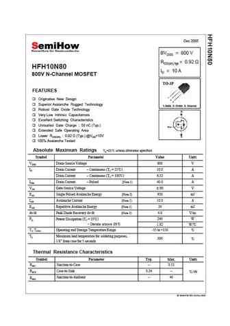
Dec 2005 BVDSS = 800 V RDS(on) typ = 0.92 HFH10N80 ID = 10 A 800V N-Channel MOSFET TO-3P FEATURES 1 Originative New Design 2 3 Superior Avalanche Rugged Technology 1.Gate 2. Drain 3. Source Robust Gate Oxide Technology Very Low Intrinsic Capacitances Excellent Switching Characteristics Unrivalled Gate Charge 58 nC (Typ.) Unrivalled Gate Charge 58 nC (Typ ) Exte... See More ⇒
hfp10n80.pdf
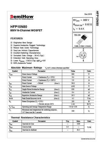
Dec 2010 BVDSS = 800 V RDS(on) typ HFP10N80 ID = 9.4 A 800V N-Channel MOSFET TO-220 FEATURES Originative New Design 1 2 3 Superior Avalanche Rugged Technology 1.Gate 2. Drain 3. Source Robust Gate Oxide Technology Very Low Intrinsic Capacitances Excellent Switching Characteristics Unrivalled Gate Charge 58 nC (Typ.) Extended Safe Operating Area Low... See More ⇒
hfs10n80.pdf
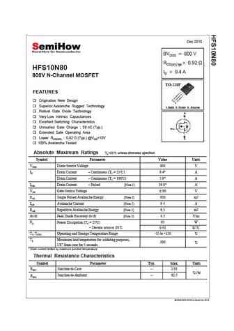
Dec 2010 BVDSS = 800 V RDS(on) typ = 0.92 HFS10N80 ID = 9.4 A 800V N-Channel MOSFET TO-220F FEATURES 1 Originative New Design 2 3 Superior Avalanche Rugged Technology 1.Gate 2. Drain 3. Source Robust Gate Oxide Technology Very Low Intrinsic Capacitances Excellent Switching Characteristics Unrivalled Gate Charge 58 nC (Typ.) Unrivalled Gate Charge 58 nC (Typ ) E... See More ⇒
hfs10n80a.pdf
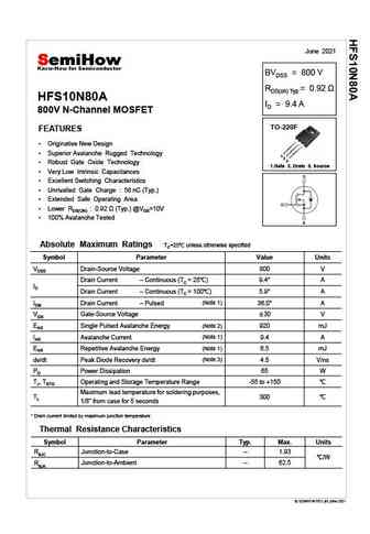
June 2021 BVDSS = 800 V RDS(on) Typ = 0.92 HFS10N80A ID = 9.4 A 800V N-Channel MOSFET TO-220F FEATURES Originative New Design Superior Avalanche Rugged Technology 1 2 3 Robust Gate Oxide Technology 1.Gate 2. Drain 3. Source Very Low Intrinsic Capacitances Excellent Switching Characteristics Unrivalled Gate Charge 58 nC (Typ.) Extended Safe Ope... See More ⇒
tmp10n80 tmpf10n80.pdf
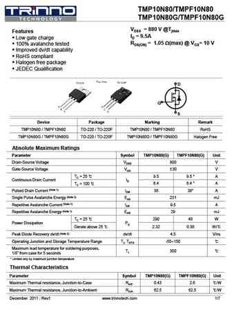
TMP10N80/TMPF10N80 TMP10N80G/TMPF10N80G VDSS = 880 V @Tjmax Features ID = 9.5A Low gate charge RDS(ON) = 1.05 W(max) @ VGS= 10 V 100% avalanche tested Improved dv/dt capability RoHS compliant Halogen free package JEDEC Qualification D G S Device Package Marking Remark TMP10N80 / TMPF10N80 TO-220 / TO-220F TMP10N80 / TMPF10N80 RoHS TMP10N... See More ⇒
tman10n80.pdf
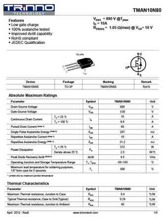
TMAN10N80 VDSS = 880 V @Tjmax Features ID = 10A Low gate charge RDS(on) = 1.05 W(max) @ VGS= 10 V 100% avalanche tested Improved dv/dt capability RoHS compliant JEDEC Qualification D G S Device Package Marking Remark TMAN10N80 TO-3P TMAN10N80 RoHS Absolute Maximum Ratings Parameter Symbol TMAN10N80 Unit Drain-Source Voltage VDS 900 V Gate-... See More ⇒
tsf10n80m.pdf
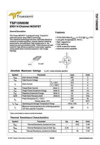
TSF10N80M 800V N-Channel MOSFET General Description Features This Power MOSFET is produced using Truesemi s 10.0A,800V,Max.RDS(on)=1.10 @ VGS =10V advanced planar stripe DMOS technology. This advanced technology has been especially tailored to Low gate charge(typical 45nC) minimize on-state resistance, provide superior switching High ruggedness performance, ... See More ⇒
wml10n80d1 wmj10n80d1.pdf
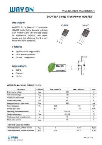
WML10N80D1 WMJ10N80D1 800V 10A 0.91 N-ch Power MOSFET Description TO-220F TO-247 WMOSTM D1 is Wayon s 1st generation TAB VDMOS family that is dramatic reduction in on-resistance and ultra-low gate charge for applications requiring high power density and high efficiency. And it is very robust and RoHS compliant. G D G S D S Features Typ.R =0.91 @V =10V DS(on) GS ... See More ⇒
wml10n80m3 wmn10n80m3 wmm10n80m3 wmo10n80m3 wmp10n80m3 wmk10n80m3.pdf
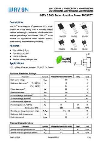
WML10N80M3, W 80M3, WM M3 WMN10N8 MM10N80M WMO1 80M3, WM M3 10N80M3, WMP10N8 MK10N80M 800V 0.86 S T V Super Junction Power MOSFET Descrip ption WMOSTM M3 is Wayo neration 800 M on s 3rd gen 0V super junction MOSFET fa that is utilizing charge M amily S balance te or extremely esistance D echnology fo y low on-re S S G D D G G G T and low ga charge perfo... See More ⇒
cs10n80fa9d.pdf
Silicon N-Channel Power MOSFET R CS10N80F A9D General Description VDSS 800 V CS10N80F A9D, the silicon N-channel Enhanced ID 10 A PD(TC=25 ) 60 W VDMOSFETs, is obtained by the self-aligned planar Technology RDS(ON)Typ 0.72 which reduce the conduction loss, improve switching performance and enhance the avalanche energy. The transistor can be used in various ... See More ⇒
cs10n80a8d.pdf
Silicon N-Channel Power MOSFET R CS10N80 A8D General Description VDSS 800 V CS10N80 A8D, the silicon N-channel Enhanced ID 10 A PD(TC=25 ) 160 W VDMOSFETs, is obtained by the self-aligned planar Technology RDS(ON)Typ 0.72 which reduce the conduction loss, improve switching performance and enhance the avalanche energy. The transistor can be used in various po... See More ⇒
cs10n80f cs10n80p cs10n80v cs10n80w.pdf
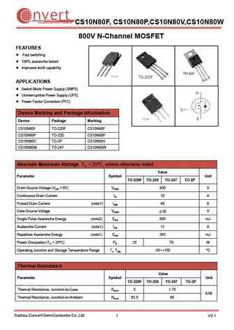
nvert Suzhou Convert Semiconductor Co ., Ltd. CS10N80F, CS10N80P,CS10N80V,CS10N80W 800V N-Channel MOSFET FEATURES Fast switching 100% avalanche tested Improved dv/dt capability APPLICATIONS Switch Mode Power Supply (SMPS) Uninterruptible Power Supply (UPS) Power Factor Correction (PFC) Device Marking and Package Information Device Package Marking CS10N80F T... See More ⇒
fir10n80fg.pdf
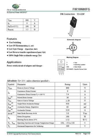
FIR10N80FG N-Channel Power MOSFET PIN Connection TO-220F VDSS 800 V ID 9 A PD(TC=25 ) 190 W RDS(ON) 1.2 G D S Features g Schematic dia ram D Fast Switching Low ON Resistance(Rdson 1.20 ) G Low Gate Charge (Typical Data 48nC) Low Reverse transfer capacitances(Typical 17pF) S 100% Single Pulse avalanche energy Test Marking Diagram Applications Y... See More ⇒
spc10n80g.pdf
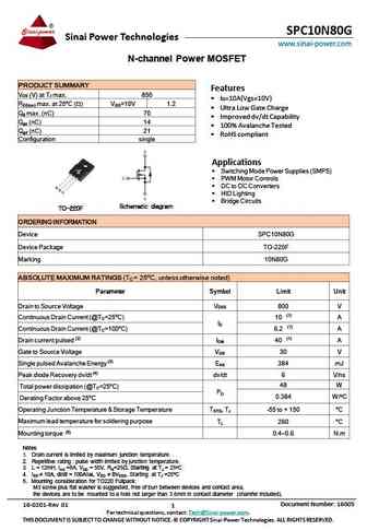
SPC10N80G Sinai Power Technologies www.sinai-power.com N-channel Power MOSFET PRODUCT SUMMARY Features V (V) at T max. 850 DS J ID=10A(Vgs=10V) R max. at 25oC ( ) V =10V 1.2 DS(on) GS Ultra Low Gate Charge Q max. (nC) 70 g Improved dv/dt Capability Q (nC) 14 gs 100% Avalanche Tested Q (nC) 21 gd RoHS compliant Configuration single A... See More ⇒
tma10n80h.pdf
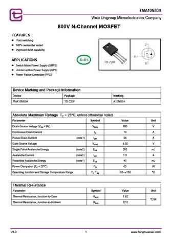
TMA10N80H Wuxi Unigroup Microelectronics Company 800V N-Channel MOSFET FEATURES Fast switching 100% avalanche tested Improved dv/dt capability APPLICATIONS Switch Mode Power Supply (SMPS) Uninterruptible Power Supply (UPS) Power Factor Correction (PFC) Device Marking and Package Information Device Package Marking TMA10N80H TO-220F A10N80H Abs... See More ⇒
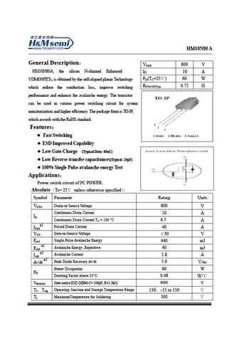
hm10n80f.pdf
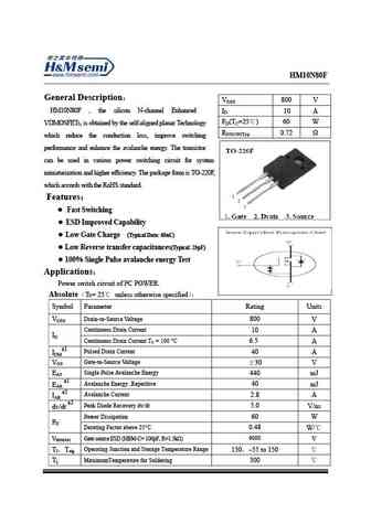
HM10N80F General Description VDSS 800 V HM10N80F , the silicon N-channel Enhanced ID 10 A PD(TC=25 ) 60 W VDMOSFETs, is obtained by the self-aligned planar Technology RDS(ON)Typ 0.72 which reduce the conduction loss, improve switching performance and enhance the avalanche energy. The transistor can be used in various power switching circuit for system miniaturizat... See More ⇒
hm10n80a.pdf
HM10N80A General Description VDSS 800 V HM10N80A, the silicon N-channel Enhanced ID 10 A PD(TC=25 ) 60 W VDMOSFETs, is obtained by the self-aligned planar Technology RDS(ON)Typ 0.72 which reduce the conduction loss, improve switching performance and enhance the avalanche energy. The transistor can be used in various power switching circuit for system miniaturizati... See More ⇒
fxn10n80f.pdf
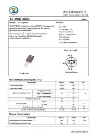
FuXin Semiconductor Co., Ltd. FXN10N80F Series Rev.A General Description Features The FXN10N80F uses advanced Silicon s MOSFET Technology, which V = 800V DS provides high performance in on-state resistance, fast switching ID = 10A @V = 10V GS performance, and excellent quality. Very low on-resistance These devices can also be utilized in industrial a... See More ⇒
10n80.pdf
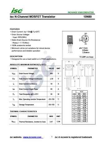
isc N-Channel MOSFET Transistor 10N80 FEATURES Drain Current I = 10A@ T =25 D C Drain Source Voltage- V = 800V(Min) DSS Static Drain-Source On-Resistance R = 1.1 (Max) DS(on) 100% avalanche tested Minimum Lot-to-Lot variations for robust device performance and reliable operation DESCRIPTION Designed for use a load switch or in PWM applications. ABSOLUTE MAX... See More ⇒
Detailed specifications: 8958, 9926, 045Y, 06N03, 10N60A, 10N60AF, 10N60H, 10N80AF, SI2302, 10N90A, 11N10, 11N10G, 11P50A, 12N50A, 12N60A, 12N60AF, 13N110A
Keywords - 10N80B MOSFET specs
10N80B cross reference
10N80B equivalent finder
10N80B pdf lookup
10N80B substitution
10N80B replacement
Can't find your MOSFET? Learn how to find a substitute transistor by analyzing voltage, current and package compatibility
History: 4800 | IRLU3714 | SRC60R022FBS | KHB9D0N90F1 | DH020N03D | PPMT2301 | S80N18R
🌐 : EN ES РУ

LIST
Last Update
MOSFET: AUB034N10 | AUB033N08BG | AUB026N085 | AUA062N08BG | AUA060N08AG | AUA056N08BGL | AUA039N10 | ASW80R290E | ASW65R120EFD | ASW65R110E
Popular searches
irfz44 | 2n5551 | irf540n | irf3205 mosfet | 2n3055 | irfp260n | 2n2222 datasheet | irf9540