11N10G Specs and Replacement
Type Designator: 11N10G
Type of Transistor: MOSFET
Type of Control Channel: N-Channel
Absolute Maximum Ratings
Pd ⓘ - Maximum Power Dissipation: 28 W
|Vds|ⓘ - Maximum Drain-Source Voltage: 100 V
|Vgs|ⓘ - Maximum Gate-Source Voltage: 20 V
|Id| ⓘ - Maximum Drain Current: 11 A
Tj ⓘ - Maximum Junction Temperature: 175 °C
Electrical Characteristics
tr ⓘ - Rise Time: 3 nS
Cossⓘ - Output Capacitance: 120 pF
RDSonⓘ - Maximum Drain-Source On-State Resistance: 0.095 Ohm
Package: TO-252
11N10G substitution
- MOSFET ⓘ Cross-Reference Search
11N10G datasheet
11n10g.pdf
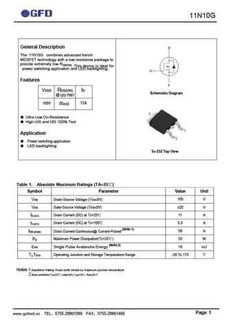
11N10G General Description The 11N10G combines advanced trench MOSFET technology with a low resistance package to provide extremely low RDS(ON) . This device is ideal for power switching application and LED backlighting. Features VDSS RDS(ON) ID Schematic Diagram @ 10V (typ) 11A 100V 85m Ultra Low On-Resistance High UIS and UIS 100% Test Application ... See More ⇒
11n10c.pdf
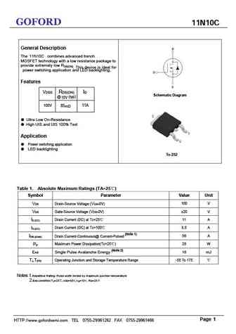
GOFORD 11N10C General Description The 11N10C combines advanced trench MOSFET technology with a low resistance package to provide extremely low RDS(ON) . This device is ideal for power switching application and LED backlighting. Features VDSS RDS(ON) ID Schematic Diagram @ 10V (typ) 11A 100V 85m Ultra Low On-Resistance High UIS and UIS 100% Test Applicatio... See More ⇒
11n10.pdf
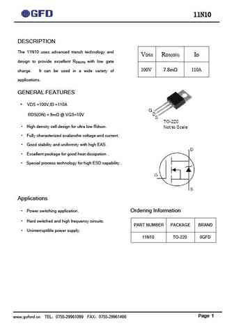
11N10 DESCRIPTION The 11N10 uses advanced trench technology and VDSS RDS(ON) ID design to provide excellent R with low gate DS(ON) 100V 7.8m 110A charge. It can be used in a wide variety of applications. GENERAL FEATURES VDS =100V,ID =110A RDS(ON) ... See More ⇒

Detailed specifications: 06N03 , 10N60A , 10N60AF , 10N60H , 10N80AF , 10N80B , 10N90A , 11N10 , 20N50 , 11P50A , 12N50A , 12N60A , 12N60AF , 13N110A , 13N60A , 13N60AF , 16N60A .
Keywords - 11N10G MOSFET specs
11N10G cross reference
11N10G equivalent finder
11N10G pdf lookup
11N10G substitution
11N10G replacement
Need a MOSFET replacement? Our guide shows you how to find a perfect substitute by comparing key parameters and specs
🌐 : EN ES РУ

LIST
Last Update
MOSFET: HAF1008S | HAF1008L | EMZB08P03H | CS30N20FA9R | AOT66613L | AOSP21313C | AOSP21311C | AOB66918L | AO3415C | AOTF20N40L
Popular searches
irf3205 mosfet | 2n3055 | irfp260n | 2n2222 datasheet | irf9540 | 2n3055 datasheet | 2sc945 | irfp250n