20N50B Specs and Replacement
Type Designator: 20N50B
Type of Transistor: MOSFET
Type of Control Channel: N-Channel
Absolute Maximum Ratings
Pd ⓘ - Maximum Power Dissipation: 280 W
|Vds|ⓘ - Maximum Drain-Source Voltage: 500 V
|Vgs|ⓘ - Maximum Gate-Source Voltage: 30 V
|Id| ⓘ - Maximum Drain Current: 20 A
Tj ⓘ - Maximum Junction Temperature: 150 °C
Electrical Characteristics
tr ⓘ - Rise Time: 375 nS
Cossⓘ - Output Capacitance: 355 pF
RDSonⓘ - Maximum Drain-Source On-State Resistance: 0.23 Ohm
Package: TO-3PB
20N50B substitution
- MOSFET ⓘ Cross-Reference Search
20N50B datasheet
20n50b.pdf
RoHS 20N50 Series RoHS SEMICONDUCTOR Nell High Power Products N-Channel Power MOSFET (20A, 500Volts) DESCRIPTION D The Nell 20N50 is a three-terminal silicon device with current conduction capability of 20A, fast switching speed, low on-state resistance, breakdown voltage rating of 500V, TO-3PB and max. threshold voltage of 5 volts. G D (20N50B) They are designed for use i... See More ⇒
mpva20n50b mpvp20n50b mpvw20n50b mpvt20n50b.pdf
MPVX20N50B Series Power MOSFET MPSW60M041 FEATURES APPLICATIONS l BVDSS 500V, ID=20A l Switch Mode Power Supply (SMPS) l RDS(on) 0.3 (Max) @VGS=10V l Uninterruptible Power Supply (UPS) l Very Low FOM (RDS(on) *Qg) l Power Factor Correction (PFC) l Excellent stability and uniformity l AC to DC Converters D G S TO-220F TO-220 TO-247 TO-3P Ordering Information Type NO. Mar... See More ⇒
mty20n50e.pdf
MOTOROLA Order this document SEMICONDUCTOR TECHNICAL DATA by MTY20N50E/D Designer's Data Sheet MTY20N50E TMOS E-FET. Motorola Preferred Device Power Field Effect Transistor N Channel Enhancement Mode Silicon Gate TMOS POWER FET This high voltage MOSFET uses an advanced termination 20 AMPERES scheme to provide enhanced voltage blocking capability without 500 VOLTS degr... See More ⇒
mtw20n50e.pdf
MOTOROLA Order this document SEMICONDUCTOR TECHNICAL DATA by MTW20N50E/D Designer's Data Sheet MTW20N50E TMOS E-FET. Motorola Preferred Device Power Field Effect Transistor TO-247 with Isolated Mounting Hole TMOS POWER FET N Channel Enhancement Mode Silicon Gate 20 AMPERES 500 VOLTS This high voltage MOSFET uses an advanced termination RDS(on) = 0.24 OHM scheme to provi... See More ⇒
mtw20n50erev4.pdf

MOTOROLA Order this document SEMICONDUCTOR TECHNICAL DATA by MTW20N50E/D Designer's Data Sheet MTW20N50E TMOS E-FET. Motorola Preferred Device Power Field Effect Transistor TO-247 with Isolated Mounting Hole TMOS POWER FET N Channel Enhancement Mode Silicon Gate 20 AMPERES 500 VOLTS This high voltage MOSFET uses an advanced termination RDS(on) = 0.24 OHM scheme to provi... See More ⇒
mtv20n50e.pdf
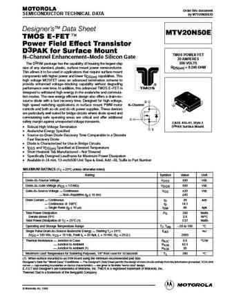
MOTOROLA Order this document SEMICONDUCTOR TECHNICAL DATA by MTV20N50E/D Designer's Data Sheet MTV20N50E TMOS E-FET. Power Field Effect Transistor D3PAK for Surface Mount TMOS POWER FET N Channel Enhancement Mode Silicon Gate 20 AMPERES 500 VOLTS The D3PAK package has the capability of housing the largest chip RDS(on) = 0.240 OHM size of any standard, plastic, surface m... See More ⇒
irfb20n50k.pdf
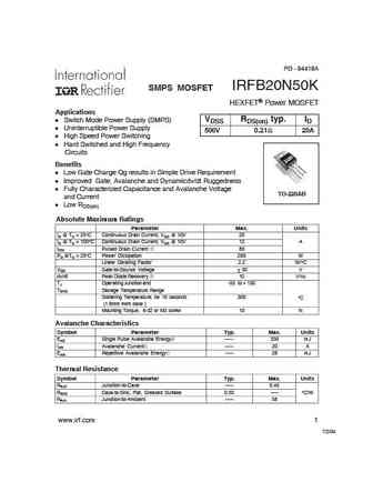
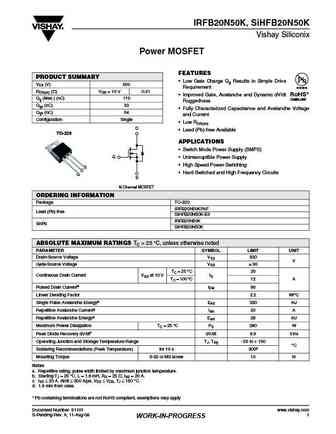
PD - 94418A IRFB20N50K SMPS MOSFET HEXFET Power MOSFET Applications VDSS RDS(on) typ. ID l Switch Mode Power Supply (SMPS) l Uninterruptible Power Supply 500V 0.21 20A l High Speed Power Switching l Hard Switched and High Frequency Circuits Benefits l Low Gate Charge Qg results in Simple Drive Requirement l Improved Gate, Avalanche and Dynamicdv/dt Ruggedness l Fully Charact... See More ⇒
irfb20n50kpbf.pdf
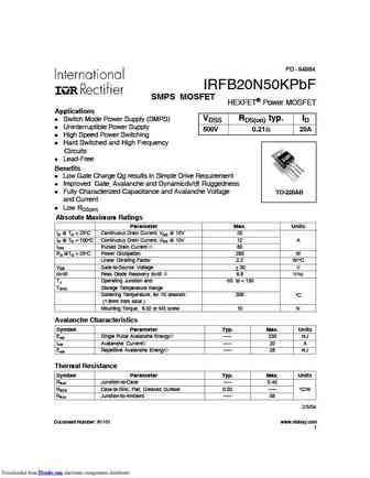
PD - 94984 IRFB20N50KPbF SMPS MOSFET HEXFET Power MOSFET AppIications VDSS RDS(on) typ. ID l Switch Mode Power Supply (SMPS) l Uninterruptible Power Supply 500V 0.21 20A l High Speed Power Switching l Hard Switched and High Frequency Circuits l Lead-Free Benefits l Low Gate Charge Qg results in Simple Drive Requirement l Improved Gate, Avalanche and Dynamicdv/dt Ruggedness ... See More ⇒
phw20n50e 2.pdf
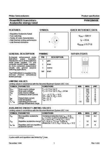
Philips Semiconductors Product specification PowerMOS transistors PHW20N50E Avalanche energy rated FEATURES SYMBOL QUICK REFERENCE DATA d Repetitive Avalanche Rated Fast switching VDSS = 500 V Stable off-state characteristics High thermal cycling performance ID = 20 A g Low thermal resistance RDS(ON) 0.27 s GENERAL DESCRIPTION PINNING SOT429 (TO247) ... See More ⇒
fdp20n50f fdpf20n50ft.pdf
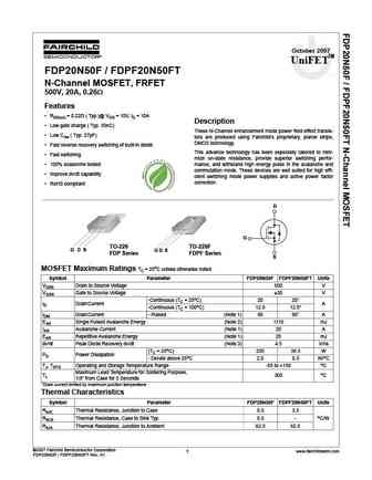
October 2007 UniFETTM FDP20N50F / FDPF20N50FT tm N-Channel MOSFET, FRFET 500V, 20A, 0.26 Features RDS(on) = 0.22 ( Typ.)@ VGS = 10V, ID = 10A Description Low gate charge ( Typ. 50nC) These N-Channel enhancement mode power field effect transis- Low Crss ( Typ. 27pF) tors are produced using Fairchild s proprietary, planar stripe, DMOS technology. Fast reve... See More ⇒
fdp20n50 fdpf20n50.pdf
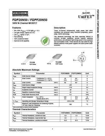
April 2007 TM UniFET FDP20N50 / FDPF20N50 500V N-Channel MOSFET Features Description 20A, 500V, RDS(on) = 0.23 @VGS = 10 V These N-Channel enhancement mode power field effect transistors are produced using Fairchild s proprietary, planar Low gate charge ( typical 45.6 nC) stripe, DMOS technology. Low Crss ( typical 27 pF) This advanced technology has been especially... See More ⇒
fdp20n50 fdpf20n50 fdpf20n50t.pdf
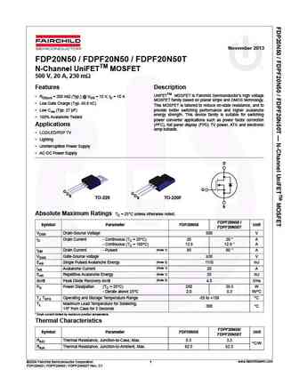
November 2013 FDP20N50 / FDPF20N50 / FDPF20N50T N-Channel UniFETTM MOSFET 500 V, 20 A, 230 m Features Description UniFETTM MOSFET is Fairchild Semiconductor s high voltage RDS(on) = 200 m (Typ.) @ VGS = 10 V, ID = 10 A MOSFET family based on planar stripe and DMOS technology. Low Gate Charge (Typ. 45.6 nC) This MOSFET is tailored to reduce on-state resistance, and to ... See More ⇒
fda20n50f.pdf
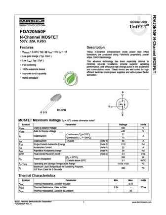
October 2007 UniFETTM FDA20N50F tm N-Channel MOSFET 500V, 22A, 0.26 Features Description RDS(on) = 0.22 ( Typ.) @ VGS = 10V, ID = 11A These N-Channel enhancement mode power field effect transistors are produced using Failchild s proprietary, planar Low gate charge ( Typ. 50nC ) stripe, DMOS technology. Low Crss ( Typ. 27pF ) This advance technology has been es... See More ⇒
fda20n50 f109.pdf
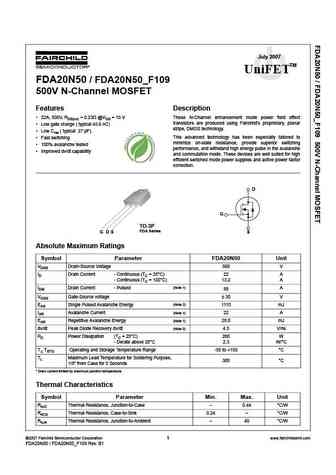
July 2007 TM UniFET FDA20N50 / FDA20N50_F109 500V N-Channel MOSFET Features Description 22A, 500V, RDS(on) = 0.23 @VGS = 10 V These N-Channel enhancement mode power field effect transistors are produced using Fairchild s proprietary, planar Low gate charge ( typical 45.6 nC) stripe, DMOS technology. Low Crss ( typical 27 pF) This advanced technology has been especial... See More ⇒
fdb20n50f.pdf
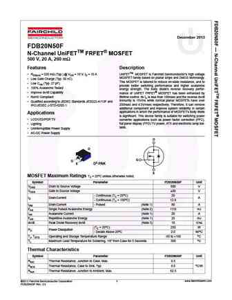
December 2013 FDB20N50F N-Channel UniFETTM FRFET MOSFET 500 V, 20 A, 260 m Features Description RDS(on) = 220 m (Typ.) @ VGS = 10 V, ID = 10 A UniFETTM MOSFET is Fairchild Semiconductor s high voltage MOSFET family based on planar stripe and DMOS technology. Low Gate Charge (Typ. 50 nC) This MOSFET is tailored to reduce on-state resistance, and to Low Crss (Typ. 27... See More ⇒
rdx120n50fu6.pdf
RDX120N50 Transistors 10V Drive Nch MOS FET RDX120N50 Structure External dimensions (Unit mm) Silicon N-channel MOS FET TO-220FM 10.0 3.2 4.5 2.8 Features 1) Low on-resistance. 2) Low input capacitance. 1.2 1.3 3) Excellent resistance to damage from static electricity. 0.8 (1)Gate 2.54 2.54 0.75 2.6 (2)Drain (1) (2) (3) Applications (3)Source Switching ... See More ⇒
sihg20n50c.pdf

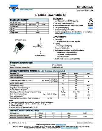
SiHG20N50C Vishay Siliconix Power MOSFET FEATURES PRODUCT SUMMARY Halogen-free According to IEC 61249-2-21 VDS (V) at TJ max. 560 Definition RDS(on) ( )VGS = 10 V 0.270 Low Figure-of-Merit Ron x Qg Qg (Max.) (nC) 76 100 % Avalanche Tested Qgs (nC) 21 High Peak Current Capability Qgd (nC) 34 dV/dt Ruggedness Configuration Single Improved Trr/Qrr Imp... See More ⇒
sihs20n50c.pdf

SiHS20N50C Vishay Siliconix Power MOSFET FEATURES PRODUCT SUMMARY Low Figure-of-Merit Ron x Qg VDS (V) at TJ max. 560 100 % Avalanche Tested RDS(on) ( )VGS = 10 V 0.270 High Peak Current Capability Qg (Max.) (nC) 76 dV/dt Ruggedness Qgs (nC) 21 Improved trr/Qrr Qgd (nC) 34 Improved Gate Charge Configuration Single High Power Dissipations Capability... See More ⇒
sihp20n50e.pdf

SiHP20N50E www.vishay.com Vishay Siliconix E Series Power MOSFET FEATURES PRODUCT SUMMARY Low figure-of-merit (FOM) Ron x Qg VDS (V) at TJ max. 550 Low input capacitance (Ciss) RDS(on) max. at 25 C ( ) VGS = 10 V 0.184 Reduced switching and conduction losses Qg max. (nC) 92 Low gate charge (Qg) Qgs (nC) 10 Avalanche energy rated (UIS) Qgd (nC) 19 Mater... See More ⇒
sihb20n50e.pdf
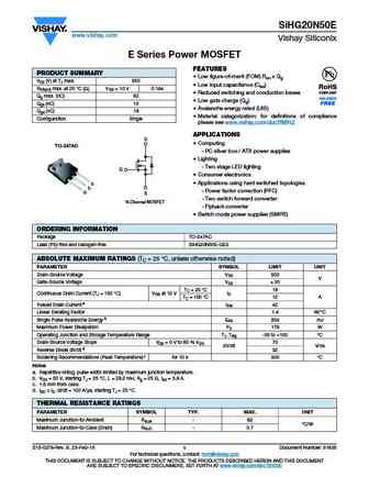
SiHB20N50E www.vishay.com Vishay Siliconix E Series Power MOSFET FEATURES PRODUCT SUMMARY Low figure-of-merit (FOM) Ron x Qg VDS (V) at TJ max. 550 Low input capacitance (Ciss) RDS(on) max. at 25 C ( ) VGS = 10 V 0.184 Reduced switching and conduction losses Qg max. (nC) 92 Low gate charge (Qg) Qgs (nC) 10 Avalanche energy rated (UIS) Qgd (nC) 19 Mater... See More ⇒
irfb20n50k sihfb20n50k.pdf
IRFB20N50K, SiHFB20N50K Vishay Siliconix Power MOSFET FEATURES PRODUCT SUMMARY Low Gate Charge Qg Results in Simple Drive VDS (V) 500 Requirement Available RDS(on) ( )VGS = 10 V 0.21 Improved Gate, Avalanche and Dynamic dV/dt RoHS* Qg (Max.) (nC) 110 COMPLIANT Ruggedness Qgs (nC) 33 Fully Characterized Capacitance and Avalanche Voltage Qgd (nC) 54 and Current Conf... See More ⇒
siha20n50e.pdf

SiHA20N50E www.vishay.com Vishay Siliconix E Series Power MOSFET FEATURES PRODUCT SUMMARY Low figure-of-merit (FOM) Ron x Qg VDS (V) at TJ max. 550 Low input capacitance (Ciss) RDS(on) max. at 25 C ( ) VGS = 10 V 0.184 Reduced switching and conduction losses Qg max. (nC) 92 Low gate charge (Qg) Qgs (nC) 10 Avalanche energy rated (UIS) Qgd (nC) 19 Mater... See More ⇒
sihg20n50e.pdf
SiHG20N50E www.vishay.com Vishay Siliconix E Series Power MOSFET FEATURES PRODUCT SUMMARY Low figure-of-merit (FOM) Ron x Qg VDS (V) at TJ max. 550 Low input capacitance (Ciss) RDS(on) max. at 25 C ( ) VGS = 10 V 0.184 Reduced switching and conduction losses Qg max. (nC) 92 Low gate charge (Qg) Qgs (nC) 10 Avalanche energy rated (UIS) Qgd (nC) 19 Mater... See More ⇒
ixfa20n50p3 ixfh20n50p3 ixfp20n50p3 ixfq20n50p3.pdf
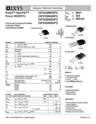
Advance Technical Information Polar3TM HiperFETTM VDSS = 500V IXFA20N50P3 ID25 = 20A Power MOSFETs IXFP20N50P3 RDS(on) 300m IXFQ20N50P3 N-Channel Enhancement Mode IXFH20N50P3 Avalanche Rated TO-220AB (IXFP) Fast Intrinsic Rectifier TO-263 AA (IXFA) G G D D (Tab) S S TO-3P (IXFQ) D (Tab) Symbol Test Conditions Maximum Ratings G VDSS TJ... See More ⇒
ixfp20n50p3m.pdf
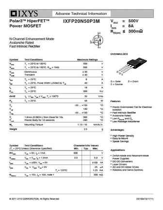
Advance Technical Information Polar3TM HiperFETTM VDSS = 500V IXFP20N50P3M Power MOSFET ID25 = 8A RDS(on) 300m N-Channel Enhancement Mode Avalanche Rated Fast Intrinsic Rectifier OVERMOLDED Symbol Test Conditions Maximum Ratings VDSS TJ = 25 C to 150 C 500 V VDGR TJ = 25 C to 150 C, RGS = 1M 500 V VGSS Continuous 30 V G D S VGSM Tran... See More ⇒
fdp20n50f fdpf20n50ft.pdf

Is Now Part of To learn more about ON Semiconductor, please visit our website at www.onsemi.com Please note As part of the Fairchild Semiconductor integration, some of the Fairchild orderable part numbers will need to change in order to meet ON Semiconductor s system requirements. Since the ON Semiconductor product management systems do not have the ability to manage part nomenclatur... See More ⇒
mtw20n50e.pdf
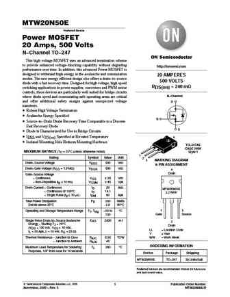
MTW20N50E Preferred Device Power MOSFET 20 Amps, 500 Volts N Channel TO 247 This high voltage MOSFET uses an advanced termination scheme to provide enhanced voltage blocking capability without degrading http //onsemi.com performance over time. In addition, this advanced Power MOSFET is designed to withstand high energy in the avalanche and commutation 20 AMPERES modes. The new ... See More ⇒
fdp20n50 fdpf20n50 fdpf20n50t.pdf

Is Now Part of To learn more about ON Semiconductor, please visit our website at www.onsemi.com Please note As part of the Fairchild Semiconductor integration, some of the Fairchild orderable part numbers will need to change in order to meet ON Semiconductor s system requirements. Since the ON Semiconductor product management systems do not have the ability to manage part nomenclatur... See More ⇒
fdb20n50f.pdf

Is Now Part of To learn more about ON Semiconductor, please visit our website at www.onsemi.com Please note As part of the Fairchild Semiconductor integration, some of the Fairchild orderable part numbers will need to change in order to meet ON Semiconductor s system requirements. Since the ON Semiconductor product management systems do not have the ability to manage part nomenclatur... See More ⇒
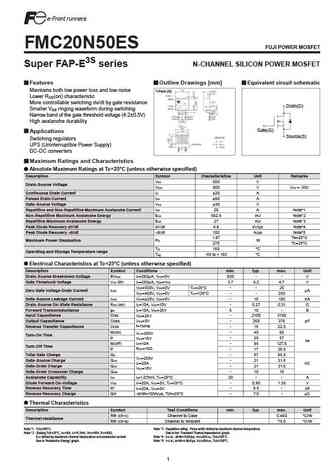
fmh20n50es.pdf
FMH20N50ES FUJI POWER MOSFET Super FAP-E3S series N-CHANNEL SILICON POWER MOSFET Features Outline Drawings [mm] Equivalent circuit schematic Maintains both low power loss and low noise TO-3P (Q) Lower R (on) characteristic DS More controllable switching dv/dt by gate resistance Drain(D) Smaller V ringing waveform during switching GS Narrow band of the gate threshold voltage (4.2 0.5... See More ⇒
fmc20n50es.pdf
FMC20N50ES FUJI POWER MOSFET Super FAP-E3S series N-CHANNEL SILICON POWER MOSFET Features Outline Drawings [mm] Equivalent circuit schematic Maintains both low power loss and low noise T-Pack (S) Lower R (on) characteristic DS More controllable switching dv/dt by gate resistance Drain(D) Smaller V ringing waveform during switching GS Narrow band of the gate threshold voltage (4.2 0.... See More ⇒
fmp20n50es.pdf

FMP20N50ES FUJI POWER MOSFET Super FAP-E3S series N-CHANNEL SILICON POWER MOSFET Features Outline Drawings [mm] Equivalent circuit schematic Maintains both low power loss and low noise TO-220AB Lower R (on) characteristic DS More controllable switching dv/dt by gate resistance Drain(D) Smaller V ringing waveform during switching GS Narrow band of the gate threshold voltage (4.2 0.5V... See More ⇒
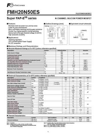
fmh20n50e.pdf
FMH20N50E FUJI POWER MOSFET Super FAP-E3 series N-CHANNEL SILICON POWER MOSFET Features Outline Drawings [mm] Equivalent circuit schematic Maintains both low power loss and low noise TO-3P(Q) Lower R (on) characteristic DS More controllable switching dv/dt by gate resistance Drain(D) Smaller V ringing waveform during switching GS Narrow band of the gate threshold voltage (3.0 0.5V) ... See More ⇒
fmc20n50e.pdf
FMC20N50E FUJI POWER MOSFET Super FAP-E3 series N-CHANNEL SILICON POWER MOSFET Features Outline Drawings [mm] Equivalent circuit schematic Maintains both low power loss and low noise T-Pack(S) Lower R (on) characteristic DS More controllable switching dv/dt by gate resistance Drain(D) Smaller V ringing waveform during switching GS Narrow band of the gate threshold voltage (3.0 0.5V)... See More ⇒
fml20n50es.pdf
http //www.fujisemi.com FML20N50ES FUJI POWER MOSFET Super FAP-E3 series N-CHANNEL SILICON POWER MOSFET Features Outline Drawings [mm] Equivalent circuit schematic Maintains both low power loss and low noise TFP 9.0 0.2 7.0 0.2 0.4 0.1 Lower R (on) characteristic DS 4 More controllable switching dv/dt by gate resistance 4 D Smaller V ringing waveform during switching GS Narrow... See More ⇒
fmp20n50e.pdf
FMP20N50E FUJI POWER MOSFET Super FAP-E3 series N-CHANNEL SILICON POWER MOSFET Features Outline Drawings [mm] Equivalent circuit schematic Maintains both low power loss and low noise TO-220AB Lower R (on) characteristic DS More controllable switching dv/dt by gate resistance Drain(D) Smaller V ringing waveform during switching GS Narrow band of the gate threshold voltage (3.0 0.5V) ... See More ⇒
fmi20n50es.pdf
FMI20N50ES FUJI POWER MOSFET Super FAP-E3S series N-CHANNEL SILICON POWER MOSFET Features Outline Drawings [mm] Equivalent circuit schematic Maintains both low power loss and low noise T-Pack (L) Lower R (on) characteristic DS More controllable switching dv/dt by gate resistance Drain(D) Smaller V ringing waveform during switching GS Narrow band of the gate threshold voltage (4.2 0.... See More ⇒
fmi20n50e.pdf
FMI20N50E FUJI POWER MOSFET Super FAP-E3 series N-CHANNEL SILICON POWER MOSFET Features Outline Drawings [mm] Equivalent circuit schematic Maintains both low power loss and low noise T-Pack(L) Lower R (on) characteristic DS More controllable switching dv/dt by gate resistance Drain(D) Smaller V ringing waveform during switching GS Narrow band of the gate threshold voltage (3.0 0.5V)... See More ⇒
fmv20n50e.pdf
FMV20N50E FUJI POWER MOSFET Super FAP-E3 series N-CHANNEL SILICON POWER MOSFET Features Outline Drawings [mm] Equivalent circuit schematic Maintains both low power loss and low noise TO-220F(SLS) Lower R (on) characteristic DS More controllable switching dv/dt by gate resistance Drain(D) Smaller V ringing waveform during switching GS Narrow band of the gate threshold voltage (3.0 0.... See More ⇒
fmv20n50es.pdf
FMV20N50ES FUJI POWER MOSFET Super FAP-E3S series N-CHANNEL SILICON POWER MOSFET Features Outline Drawings [mm] Equivalent circuit schematic Maintains both low power loss and low noise TO-220F (SLS) Lower R (on) characteristic DS More controllable switching dv/dt by gate resistance Drain(D) Smaller V ringing waveform during switching GS Narrow band of the gate threshold voltage (4.2... See More ⇒
tsm20n50ci tsm20n50cz.pdf
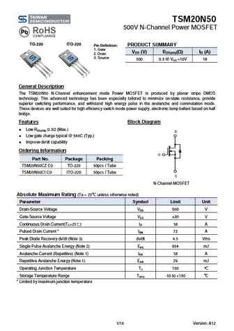
TSM20N50 500V N-Channel Power MOSFET TO-220 ITO-220 PRODUCT SUMMARY Pin Definition 1. Gate VDS (V) RDS(on)( ) ID (A) 2. Drain 3. Source 500 0.3 @ VGS =10V 18 General Description The TSM20N50 N-Channel enhancement mode Power MOSFET is produced by planar stripe DMOS technology. This advanced technology has been especially tailored to minimize on-state resistance, prov... See More ⇒
20n50.pdf
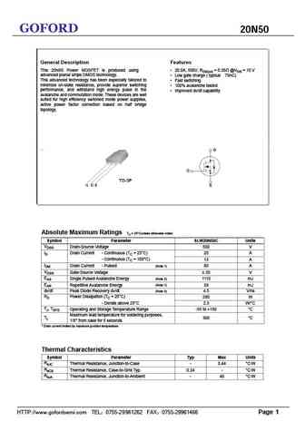
GOFORD 20N50 General Description Features This 20N50 Power MOSFET is produced using 20.0A, 500V, RDS(on) = 0.26 @VGS = 10 V advanced planar stripe DMOS technology. Low gate charge ( typical 70nC) This advanced technology has been especially tailored to Fast switching minimize on-state resistance, provide superior switching 100% avalanche tested performance, and with... See More ⇒
ssf20n50uh.pdf
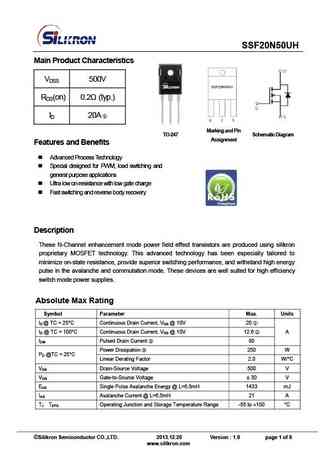
SSF20N50UH Main Product Characteristics VDSS 500V RDS(on) 0.2 (typ.) ID 20A Marking and Pi n TO-247 Schematic Diagram Assignment Features and Benefits Advanced Process Technology Special designed for PWM, load switching and general purpose applications Ultra low on-resistance with low gate charge Fast switching and reverse body recovery Descri... See More ⇒
ftw20n50a.pdf
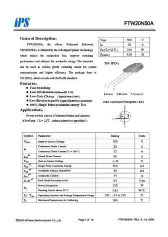
FTW20N50A General Description VDSS 500 V FTW20N50A, the silicon N-channel Enhanced ID 20 A PD (TC=25 ) 230 W VDMOSFETs, is obtained by the self-aligned planar Technology RDS(ON) 0.26 which reduce the conduction loss, improve switching performance and enhance the avalanche energy. The transistor TO 3P(N) can be used in various power switching circuit for system miniaturiz... See More ⇒
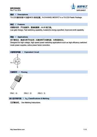
brf20n50.pdf
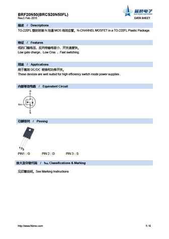
BRF20N50(BRCS20N50FL) Rev.C Feb.-2015 DATA SHEET / Descriptions TO-220FL N MOS N-CHANNEL MOSFET in a TO-220FL Plastic Package. / Features Low gate charge Low Crss Fast switching. / Applications DC/DC These devices a... See More ⇒
brfl20n50.pdf
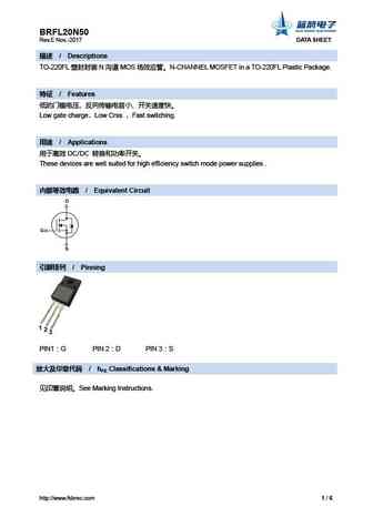
BRFL20N50 Rev.E Nov.-2017 DATA SHEET / Descriptions TO-220FL N MOS N-CHANNEL MOSFET in a TO-220FL Plastic Package. / Features Low gate charge Low Crss Fast switching. / Applications DC/DC These devices are well suit... See More ⇒
hfh20n50.pdf
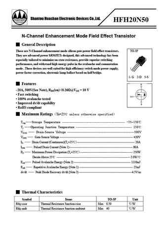
Shantou Huashan Electronic Devices Co.,Ltd. HFH20N50 N-Channel Enhancement Mode Field Effect Transistor General Description These are N-Channel enhancement mode silicon gate power field effect transistors. TO-3P They are advanced power MOSFETs designed, this advanced technology has been especially tailored to minimize on-state resistance, provide superior switching performanc... See More ⇒
cs20n50 a8h.pdf
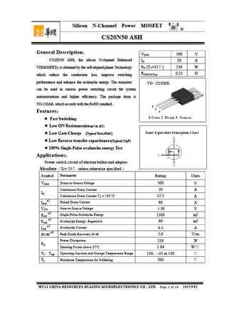
Silicon N-Channel Power MOSFET R CS20N50 A8H General Description VDSS 500 V CS20N50 A8H, the silicon N-channel Enhanced ID 20 A PD (TC=25 ) 230 W VDMOSFETs, is obtained by the self-aligned planar Technology RDS(ON)Typ 0.25 which reduce the conduction loss, improve switching performance and enhance the avalanche energy. The transistor can be used in various p... See More ⇒
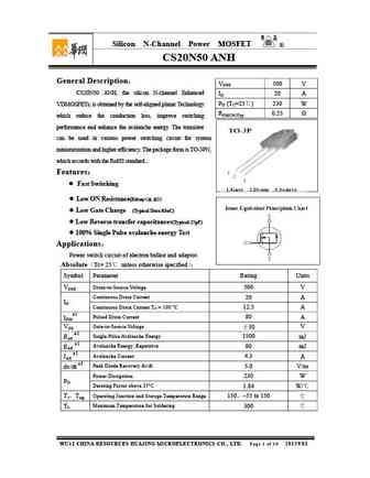
cs20n50 anh.pdf

Silicon N-Channel Power MOSFET R CS20N50 ANH General Description VDSS 500 V CS20N50 ANH, the silicon N-channel Enhanced ID 20 A PD (TC=25 ) 230 W VDMOSFETs, is obtained by the self-aligned planar Technology RDS(ON)Typ 0.25 which reduce the conduction loss, improve switching performance and enhance the avalanche energy. The transistor can be used in various po... See More ⇒

cm20n50.pdf
R CM20N50 www.jdsemi.cn ShenZhen Jingdao Electronic Co.,Ltd. POWER MOSFET 500V N-Channel VDMOS RoHS 1 2 3 ... See More ⇒
cm20n50pz.pdf

R C2N0Z M05P www.jdsemi.cn ShenZhen Jingdao Electronic Co.,Ltd. POWER MOSFET 500V N-Channel VDMOS RoHS 1 2 1 2 3 3... See More ⇒
f20n50.pdf
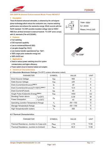
F20N50 20A 500V N-channel Enhancement Mode Power MOSFET 1 Description These N-channel enhanced vdmosfets, is obtained by the self-aligned V DSS = 500V planar technology which reduce the conduction loss, improve switching I = 20.0A D performance and enhance the avalanche energy. Which accords with the RoHS standard. TO-220F provides insulation voltage rated at 2000V R DS(on) TYP) ... See More ⇒
20n50 f20n50 i20n50 e20n50.pdf
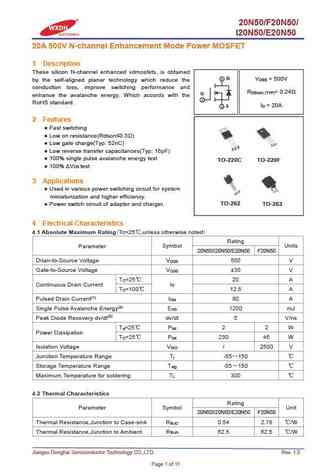
20N50/F20N50/ I20N50/E20N50 20A 500V N-channel Enhancement Mode Power MOSFET 1 Description These silicon N-channel enhanced vdmosfets, is obtained 2 D V = 500V DSS by the self-aligned planar technology which reduce the conduction loss, improve switching performance and R = 0.24 DS(on) (TYP) G enhance the avalanche energy. Which accords with the 1 RoHS standard. I = 20A 3 S D ... See More ⇒
svf20n50f svf20n50pn.pdf
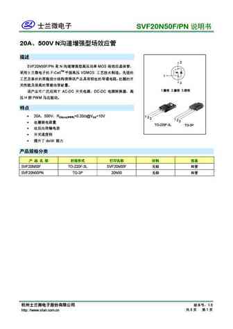
SVF20N50F/PN 20A 500V N 2 SVF20N50F/PN N MOS F-CellTM VDMOS 1 3 ... See More ⇒
msw20n50.pdf
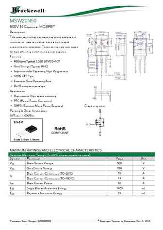
MSW20N50 500V N-Channel MOSFET Description This latest technology has been especially designed to minimize on-state resistance, have a high rugged avalanche characteristics. These devices are well suited for high efficiency switch mode power supplies. Features RDS(on) (Typical 0.26 )@VGS=10V Gate Charge (Typical 90nC) Improved dv/dt Capability, High Ruggedness ... See More ⇒
msf20n50.pdf

MSF20N50 N-Channel Enhancement Mode Power MOSFET Description The MSF20N50 is a N-channel enhancement-mode MOSFET , providing the designer with the best combination of fast switching, ruggedized device design, low on-resistance and cost effectiveness. The TO-220F package is universally preferred for all commercial-industrial applications Features Low On Resistance S... See More ⇒
bl20n50-p bl20n50-a bl20n50-w bl20n50-k.pdf
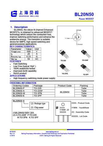
BL20N50 Power MOSFET 1 Description BL20N50, the silicon N-channel Enhanced MOSFETs, is obtained by advanced MOSFET technology which reduce the conduction loss, improve switching performance and enhance the avalanche energy. The transistor is suitable device for SMPS, high speed switching and general purpose applications. KEY CHARACTERISTICS Parameter Value Unit V 500 ... See More ⇒
jfam20n50d.pdf
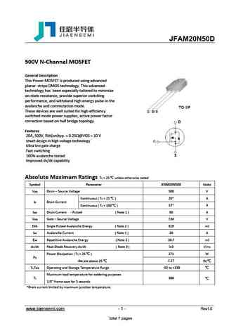
JFAM20N50D 500V N-Channel MOSFET General Description This Power MOSFET is produced using advanced planar stripe DMOS technology. This advanced technology has been especially tailored to minimize on-state resistance, provide superior switching performance, and withstand high energy pulse in the avalanche and commutation mode. These devices are well suited for high efficiency ... See More ⇒
jfpc20n50c jffm20n50c.pdf
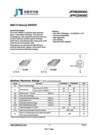
JFFM20N50C JFPC20N50C 500V N-Channel MOSFET General Description Features This Power MOSFET is produced using advanced - 20A, 500V, RDS(on)typ. = 0.21 @VGS = 10 V planar stripe DMOS technology. This advanced - Low gate charge(40nC) technology has been especially tailored to minimize - High ruggedness on-state resistance, provide superior switching - Fast switching perf... See More ⇒
jfam20n50c.pdf
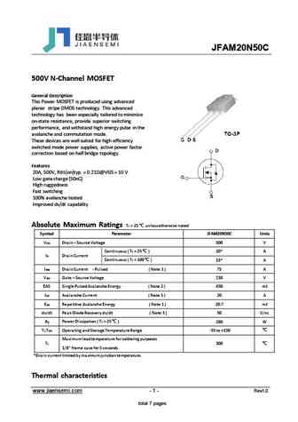
JFAM20N50C 500V N-Channel MOSFET General Description This Power MOSFET is produced using advanced planar stripe DMOS technology. This advanced technology has been especially tailored to minimize on-state resistance, provide superior switching performance, and withstand high energy pulse in the avalanche and commutation mode. These devices are well suited for high efficiency ... See More ⇒
jfam20n50e.pdf

JFAM20N50E 500V N-Channel MOSFET General Description This Power MOSFET is produced using advanced planar stripe DMOS technology. This advanced technology has been especially tailored to minimize on-state resistance, provide superior switching performance, and withstand high energy pulse in the avalanche and commutation mode. These devices are well suited for high efficiency ... See More ⇒
kia20n50h.pdf
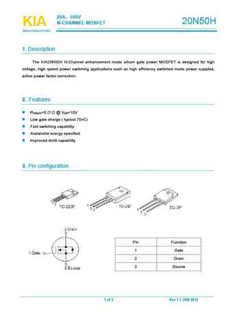
20A 500V 20N50H N-CHANNELMOSFET KIA KIA KIA SEMICONDUCTORS SEMICONDUCTORS SEMICONDUCTORS 1.Description The KIA20N50H N-Channel enhancement mode silicon gate power MOSFET is designed for high voltage, high speed power switching applications such as high efficiency switched mode power supplies, active power factor correction. 2. Features R =0.21 @V =10V DS(on) GS Lowgate ch... See More ⇒
slp20n50c slf20n50c.pdf
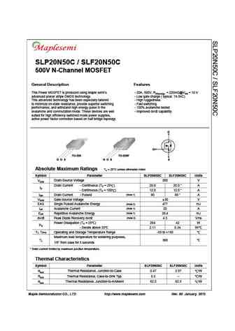
SLP20N50C / SLF20N50C 500V N-Channel MOSFET General Description Features This Power MOSFET is produced using Maple semi s - 20A, 500V, RDS(on)typ. = 220m @VGS = 10 V advanced planar stripe DMOS technology. - Low gate charge ( typical 74.5nC) This advanced technology has been especially tailored - High ruggedness to minimize on-state resistance, provide superior switching - Fast switchi... See More ⇒
slw20n50c.pdf
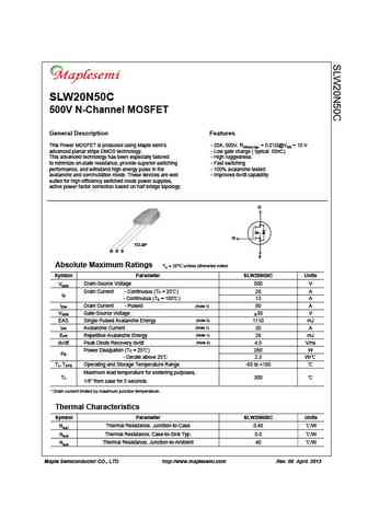
SLW20N50C 500V N-Channel MOSFET General Description Features This Power MOSFET is produced using Maple semi s - 20A, 500V, RDS(on) typ. = 0.21 @VGS = 10 V advanced planar stripe DMOS technology. - Low gate charge ( typical 50nC) This advanced technology has been especially tailored - High ruggedness to minimize on-state resistance, provide superior switching - Fast switching performan... See More ⇒
ptp20n50a pta20n50a.pdf
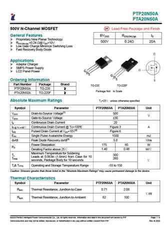
PTP20N50A PTA20N50A 500V N-Channel MOSFET General Features BVDSS RDS(ON),typ. ID Proprietary New Planar Technology 500V 0.24 20A RDS(ON),typ.=0.24 @VGS=10V Low Gate Charge Minimize Switching Loss Fast Recovery Body Diode Applications Adaptor Charger SMPS Power Supply G LCD Panel Power D S G D S Ordering Information Part Number Package Brand T... See More ⇒
ptw20n50a.pdf
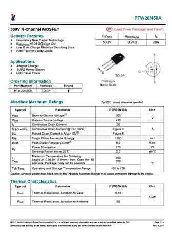
PTW20N50A 500V N-Channel MOSFET General Features BVDSS RDS(ON),typ. ID Proprietary New Planar Technology 500V 0.24 20A RDS(ON),typ.=0.24 @VGS=10V Low Gate Charge Minimize Switching Loss Fast Recovery Body Diode Applications Adaptor Charger SMPS Power Supply LCD Panel Power Ordering Information Part Number Package Brand PTW20N50A TO-3... See More ⇒
swf20n50d swt20n50d.pdf
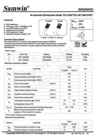
SW20N50D N-channel Enhanced mode TO-220F/TO-247 MOSFET Features TO-220F TO-247 BVDSS 500V ID 20A High ruggedness Low RDS(ON) (Typ 0.19 )@VGS=10V RDS(ON) 0.19 Low Gate Charge (Typ 82nC) Improved dv/dt Capability 2 100% Avalanche Tested 1 1 2 2 Application Charger, Adaptor, LED 3 3 1 1. Gate 2. Drain 3. Source 3 General De... See More ⇒
hfa20n50u.pdf
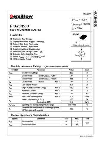
May 2014 BVDSS = 500 V RDS(on) typ HFA20N50U ID = 20 A 500V N-Channel MOSFET TO-247 FEATURES Originative New Design Superior Avalanche Rugged Technology 1 2 3 Robust Gate Oxide Technology 1.Gate 2. Drain 3. Source Very Low Intrinsic Capacitances Excellent Switching Characteristics Unrivalled Gate Charge 58 nC (Typ.) Extended Safe Operating Area L... See More ⇒
wvm20n50.pdf
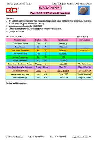
Shaanxi Qunli Electric Co., Ltd Add. No. 1 Qunli Road,Baoji City,Shaanxi,China WVM20N50 Power MOSFET(N-channel) Transistor Features 1. It s voltage control component with good input impedance, small starting power dissipation, wide area of safe operation, good temperature stability. 2. Implementation of standards QZJ840611 3. Use for high speed switch, circuit of power source co... See More ⇒
tman20n50.pdf
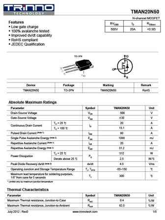
TMAN20N50 N-channel MOSFET Features BVDSS ID RDS(on) Low gate charge 500V 20A ... See More ⇒
tman20n50a.pdf
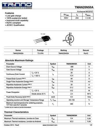
TMAN20N50A N-channel MOSFET Features BVDSS ID RDS(on) Low gate charge 100% avalanche tested 500V 20A ... See More ⇒
tmp20n50 tmpf20n50.pdf
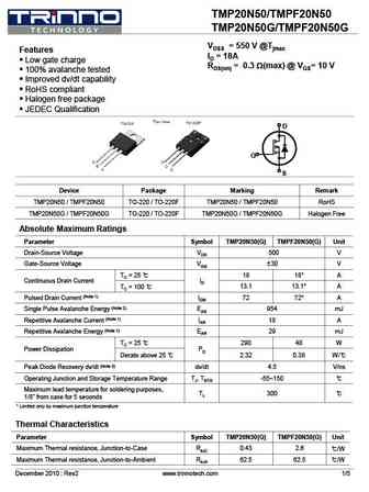
TMP20N50/TMPF20N50 TMP20N50G/TMPF20N50G VDSS = 550 V @Tjmax Features ID = 18A Low gate charge RDS(on) = 0.3 W(max) @ VGS= 10 V 100% avalanche tested Improved dv/dt capability RoHS compliant Halogen free package JEDEC Qualification D G S Device Package Marking Remark TMP20N50 / TMPF20N50 TO-220 / TO-220F TMP20N50 / TMPF20N50 RoHS TMP20N50... See More ⇒
tmp20n50a tmpf20n50a.pdf
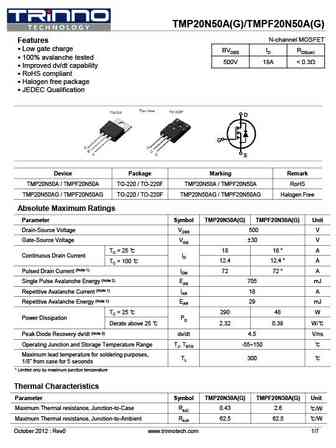
TMP20N50A(G)/TMPF20N50A(G) N-channel MOSFET Features Low gate charge BVDSS ID RDS(on) 100% avalanche tested 500V 18A ... See More ⇒
tsa20n50m.pdf
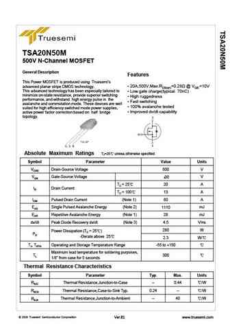
TSA20N50M 500V N-Channel MOSFET General Description Features This Power MOSFET is produced using Truesemi s 20A,500V,Max.RDS(on)=0.28 @ VGS =10V advanced planar stripe DMOS technology. This advanced technology has been especially tailored to Low gate charge(typical 70nC) minimize on-state resistance, provide superior switching High ruggedness performance, and... See More ⇒
tsf20n50m.pdf
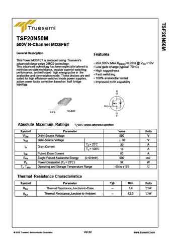
TSF20N50M 500V N-Channel MOSFET General Description Features This Power MOSFET is produced using Truesemi s 20A,500V,Max.RDS(on)=0.28 @ VGS =10V advanced planar stripe DMOS technology. This advanced technology has been especially tailored to Low gate charge(typical 70nC) minimize on-state resistance, provide superior switching High ruggedness performance, and withstan... See More ⇒
wmj20n50d1 wmk20n50d1 wml20n50d1.pdf
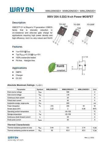
WMJ20N50D1 WMK20N50D1 WML20N50D1 500V 20A 0.22 N-ch Power MOSFET Description TO-247 TO-220 TO-220F TAB WMOSTM D1 is Wayon s 1st generation VDMOS TAB family that is dramatic reduction in on-resistance and ultra-low gate charge for applications requiring high power density and high efficiency. And it is very robust and RoHS compliant. G G G D D D S S S Features V =550V@... See More ⇒
cs20n50anh.pdf
Silicon N-Channel Power MOSFET R CS20N50 ANH General Description VDSS 500 V CS20N50 ANH, the silicon N-channel Enhanced ID 20 A PD (TC=25 ) 230 W VDMOSFETs, is obtained by the self-aligned planar Technology RDS(ON)Typ 0.25 which reduce the conduction loss, improve switching performance and enhance the avalanche energy. The transistor can be used in various po... See More ⇒
cs20n50a8h.pdf

Silicon N-Channel Power MOSFET R CS20N50 A8H General Description VDSS 500 V CS20N50 A8H, the silicon N-channel Enhanced ID 20 A PD (TC=25 ) 230 W VDMOSFETs, is obtained by the self-aligned planar Technology RDS(ON)Typ 0.25 which reduce the conduction loss, improve switching performance and enhance the avalanche energy. The transistor can be used in various p... See More ⇒
fir20n50fg.pdf
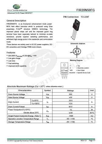
FIR20N50FG Advanced N-Ch Power MOSFET PIN Connection TO-220F General Description FIR20N50FG is an N-channel enhancement mode power MOS field effect transistor which is produced using Silan proprietary F-CellTM structure VDMOS technology. The improved planar stripe cell and the improved guard ring terminal have been especially tailored to minimize on-state resistance, provide superi... See More ⇒
ha20n50.pdf
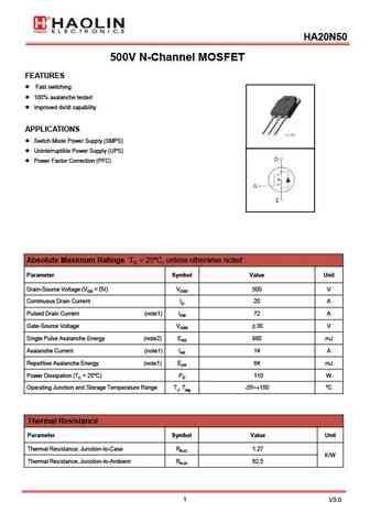
HA20N50 500V N-Channel MOSFET FEATURES Fast switching 100% avalanche tested Improved dv/dt capability APPLICATIONS Switch Mode Power Supply (SMPS) Uninterruptible Power Supply (UPS) Power Factor Correction (PFC) Absolute Maximum Ratings TC = 25 unless otherwise noted C, Parameter Symbol Value Unit Drain-Source Voltage (VGS = 0V) VDSS 500 V Continuous Drai... See More ⇒
hf20n50 hp20n50.pdf
HF20N50,HP20N50 500V N-Channel MOSFET FEATURES Fast switching 100% avalanche tested Improved dv/dt capability APPLICATIONS Switch Mode Power Supply (SMPS) Uninterruptible Power Supply (UPS) Power Factor Correction (PFC) Absolute Maximum Ratings TC = 25 unless otherwise noted C, Parameter Symbol Value Unit Drain-Source Voltage (VGS = 0V) VDSS 500 V Continu... See More ⇒
hm20n50a.pdf
500V N-Channel MOSFET General Description Features This Power MOSFET is produced using SL semi s 20.0A, 500V, RDS(on) = 0.26 @VGS = 10 V advanced planar stripe DMOS technology. Low gate charge ( typical 70nC) This advanced technology has been especially tailored to Fast switching minimize on-state resistance, provide superior switching 100% avalanche tested... See More ⇒
hm20n50f.pdf
500V N-Channel MOSFET General Description Features This Power MOSFET is produced using SL semi s 20.0A, 500V, RDS(on) = 0.26 @VGS = 10 V advanced planar stripe DMOS technology. Low gate charge ( typical 70nC) This advanced technology has been especially tailored to Fast switching minimize on-state resistance, provide superior switching 100% avalan... See More ⇒
mpf20n50.pdf
Silicon N-Channel Power MOSFET Description MPF20N50, the silicon N-channel Enhanced MOSFETS, is obtained by advanced MOSFET technology which reduce the conduction loss, improve switching performance and enhance the avalanche energy. The transistor is suitable device for Synchronous Rectification, inverter systems ,high speed switching and general purpose applications. KEY CHARACTERISTIC... See More ⇒
md20n50.pdf
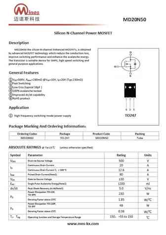
Silicon N-Channel Power MOSFET Description MD20N50 the silicon N-channel Enhanced MOSFETs, is obtained by advanced MOSFET technology which reduce the conduction loss, improve switching performance and enhance the avalanche energy. The transistor is suitable device for SMPS, high speed switching and general purpose applications. General Features V =500V, R ... See More ⇒
fxn20n50f.pdf
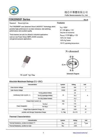
FuXin Semiconductor Co., Ltd. FXN20N50F Series Rev.A General Description Features The FXN20N50F uses advanced Silicon s MOSFET Technology, which V = 500V DS provides high performance in on-state resistance, fast switching ID = 20A @V = 10V GS performance, and excellent quality. Very low on-resistance These devices can also be utilized in industrial a... See More ⇒
mpva20n50f.pdf
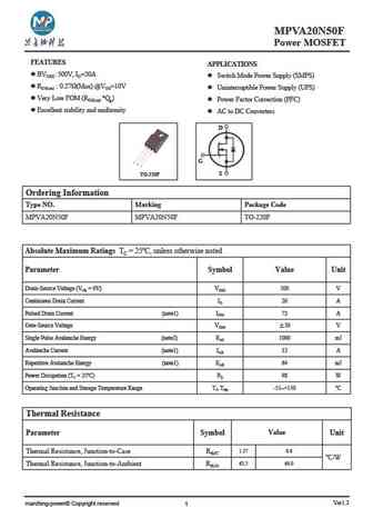
MPVA20N50F Power MOSFET MPSW60M041 FEATURES APPLICATIONS l BVDSS 500V, ID=20A l Switch Mode Power Supply (SMPS) l RDS(on) 0.27 (Max) @VGS=10V l Uninterruptible Power Supply (UPS) l Very Low FOM (RDS(on) *Qg) l Power Factor Correction (PFC) l Excellent stability and uniformity l AC to DC Converters D G S TO-220F Ordering Information Type NO. Marking Package Code MPVA20N5... See More ⇒
sihg20n50c.pdf
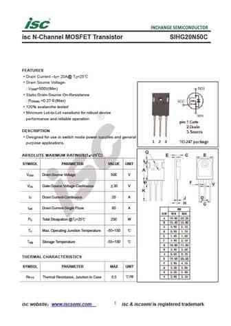
isc N-Channel MOSFET Transistor SIHG20N50C FEATURES Drain Current I = 20A@ T =25 D C Drain Source Voltage- V =500V(Min) DSS Static Drain-Source On-Resistance R =0.27 (Max) DS(on) 100% avalanche tested Minimum Lot-to-Lot variations for robust device performance and reliable operation DESCRIPTION Designed for use in switch mode power supplies and general purp... See More ⇒
fmh20n50e.pdf
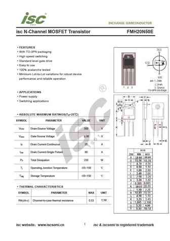
isc N-Channel MOSFET Transistor FMH20N50E FEATURES With TO-3PN packaging High speed switching Standard level gate drive Easy to use 100% avalanche tested Minimum Lot-to-Lot variations for robust device performance and reliable operation APPLICATIONS Power supply Switching applications ABSOLUTE MAXIMUM RATINGS(T =25 ) a SYMBOL PARAMETER VALUE UNIT V Drain-S... See More ⇒
fdp20n50.pdf
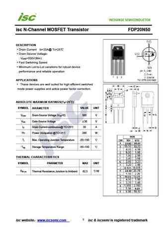
isc N-Channel MOSFET Transistor FDP20N50 DESCRIPTION Drain Current I =20A@ T =25 D C Drain Source Voltage- V =500V(Min) DSS Fast Switching Speed Minimum Lot-to-Lot variations for robust device performance and reliable operation APPLICATIONS These devices are well suited for high efficient switched mode power supplies and active power factor correction. ABSOLUTE MAXI... See More ⇒
fdb20n50f.pdf
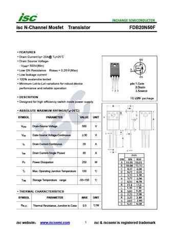
isc N-Channel Mosfet Transistor FDB20N50F FEATURES Drain Current I = 20A@ T =25 D C Drain Source Voltage- V = 500V(Min) DSS Low ON Resistance R = 0.26 (Max) DS(on) Low leakage current 100% avalanche tested Minimum Lot-to-Lot variations for robust device performance and reliable operation DESCRITION Designed for high efficiency switch mode power supply. A... See More ⇒
Detailed specifications: 16N60B, 19MT050XFAPBF, 1HN04CH, 1HP04CH, 1N60AF, 1N60E, 1N60F, 1N60G, IRF9640, 20N60A, 24N50A, 24N50B, 24N50C, 2MI50S-050, 30N20A, 38N10A, BCS4N10
Keywords - 20N50B MOSFET specs
20N50B cross reference
20N50B equivalent finder
20N50B pdf lookup
20N50B substitution
20N50B replacement
Step-by-step guide to finding a MOSFET replacement. Cross-reference parts and ensure compatibility for your repair or project.
History: WMM90R360S
🌐 : EN ES РУ

LIST
Last Update
MOSFET: AUB034N10 | AUB033N08BG | AUB026N085 | AUA062N08BG | AUA060N08AG | AUA056N08BGL | AUA039N10 | ASW80R290E | ASW65R120EFD | ASW65R110E
Popular searches
2n3055 transistor | 2n3904 datasheet | irf3710 | tip3055 | mosfet datasheet | irf3205 datasheet | irf5210 | mj15024