SFW9624 Datasheet. Specs and Replacement
Type Designator: SFW9624 📄📄
Type of Transistor: MOSFET
Type of Control Channel: P-Channel
Absolute Maximum Ratings
Pd ⓘ - Maximum Power Dissipation: 38 W
|Vds|ⓘ - Maximum Drain-Source Voltage: 250 V
|Vgs|ⓘ - Maximum Gate-Source Voltage: 30 V
|Id| ⓘ - Maximum Drain Current: 2.7 A
Tj ⓘ - Maximum Junction Temperature: 150 °C
Electrical Characteristics
tr ⓘ - Rise Time: 19 nS
Cossⓘ - Output Capacitance: 65 pF
RDSonⓘ - Maximum Drain-Source On-State Resistance: 2.4 Ohm
Package: TO263
📄📄 Copy
- MOSFET ⓘ Cross-Reference Search
SFW9624 datasheet
..1. Size:259K fairchild semi
sfi9624 sfw9624.pdf 

SFW/I9624 Advanced Power MOSFET FEATURES BVDSS = -250 V Avalanche Rugged Technology RDS(on) = 2.4 Rugged Gate Oxide Technology Lower Input Capacitance ID = -2.7 A Improved Gate Charge Extended Safe Operating Area D2-PAK I2-PAK Lower Leakage Current 10 A (Max.) @ VDS = -250V 2 Low RDS(ON) 1.65 (Typ.) 1 1 2 3 3 1. Gate 2. Drain 3. Source Absolute Maximum... See More ⇒
..2. Size:502K samsung
sfw9624.pdf

Advanced Power MOSFET FEATURES BVDSS = -250 V Avalanche Rugged Technology RDS(on) = 2.4 Rugged Gate Oxide Technology Lower Input Capacitance ID = -2.7 A Improved Gate Charge Extended Safe Operating Area Lower Leakage Current 10 A (Max.) @ VDS = -250V 2 Low RDS(ON) 1.65 (Typ.) 1 1 2 3 3 1. Gate 2. Drain 3. Source Absolute Maximum Ratings Symbol Cha... See More ⇒
8.1. Size:251K fairchild semi
sfi9620 sfw9620.pdf
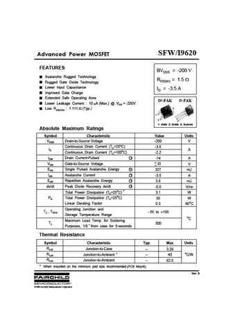
SFW/I9620 Advanced Power MOSFET FEATURES BVDSS = -200 V Avalanche Rugged Technology RDS(on) = 1.5 Rugged Gate Oxide Technology Lower Input Capacitance ID = -3.5 A Improved Gate Charge Extended Safe Operating Area D2-PAK I2-PAK Lower Leakage Current 10 A (Max.) @ VDS = -200V 2 Low RDS(ON) 1.111 (Typ.) 1 1 2 3 3 1. Gate 2. Drain 3. Source Absolute Maximu... See More ⇒
8.2. Size:504K samsung
sfw9620.pdf

Advanced Power MOSFET FEATURES BVDSS = -200 V Avalanche Rugged Technology RDS(on) = 1.5 Rugged Gate Oxide Technology Lower Input Capacitance ID = -3.5 A Improved Gate Charge Extended Safe Operating Area Lower Leakage Current 10 A (Max.) @ VDS = -200V 2 Low RDS(ON) 1.111 (Typ.) 1 1 2 3 3 1. Gate 2. Drain 3. Source Absolute Maximum Ratings Symbol Ch... See More ⇒
9.1. Size:259K fairchild semi
sfw9640tm.pdf

SFW/I9640 Advanced Power MOSFET FEATURES BVDSS = -200 V Avalanche Rugged Technology RDS(on) = 0.5 Rugged Gate Oxide Technology Lower Input Capacitance ID = -11 A Improved Gate Charge Extended Safe Operating Area D2-PAK I2-PAK Lower Leakage Current 10 A (Max.) @ VDS = -200V 2 Low RDS(ON) 0.344 (Typ.) 1 1 2 3 3 1. Gate 2. Drain 3. Source Absolute Maximum... See More ⇒
9.2. Size:256K fairchild semi
sfi9630 sfw9630.pdf

SFW/I9630 Advanced Power MOSFET FEATURES BVDSS = -200 V Avalanche Rugged Technology RDS(on) = 0.8 Rugged Gate Oxide Technology Lower Input Capacitance ID = -6.5 A Improved Gate Charge Extended Safe Operating Area D2-PAK I2-PAK Lower Leakage Current 10 A (Max.) @ VDS = -200V 2 Low RDS(ON) 0.581 (Typ.) 1 1 2 3 3 1. Gate 2. Drain 3. Source Absolute Maximu... See More ⇒
9.3. Size:263K fairchild semi
sfi9644 sfw9644.pdf

SFW/I9644 Advanced Power MOSFET FEATURES BVDSS = -250 V Avalanche Rugged Technology RDS(on) = 0.8 Rugged Gate Oxide Technology Lower Input Capacitance ID = -8.6 A Improved Gate Charge Extended Safe Operating Area D2-PAK I2-PAK Lower Leakage Current 10 A (Max.) @ VDS = -250V 2 Low RDS(ON) 0.549 (Typ.) 1 1 2 3 3 1. Gate 2. Drain 3. Source Absolute Maximu... See More ⇒
9.4. Size:254K fairchild semi
sfi9610 sfw9610.pdf

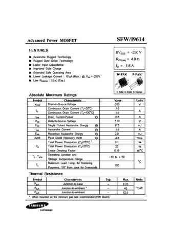
SFW/I9610 Advanced Power MOSFET FEATURES BVDSS = -200 V Avalanche Rugged Technology RDS(on) = 3.0 Rugged Gate Oxide Technology Lower Input Capacitance ID = -1.75 A Improved Gate Charge Extended Safe Operating Area D2-PAK I2-PAK Lower Leakage Current 10 A (Max.) @ VDS = -200V 2 Low RDS(ON) 2.084 (Typ.) 1 1 2 3 3 1. Gate 2. Drain 3. Source Absolute Maxi... See More ⇒
9.5. Size:264K fairchild semi
sfi9640 sfw9640.pdf

SFW/I9640 Advanced Power MOSFET FEATURES BVDSS = -200 V Avalanche Rugged Technology RDS(on) = 0.5 Rugged Gate Oxide Technology Lower Input Capacitance ID = -11 A Improved Gate Charge Extended Safe Operating Area D2-PAK I2-PAK Lower Leakage Current 10 A (Max.) @ VDS = -200V 2 Low RDS(ON) 0.344 (Typ.) 1 1 2 3 3 1. Gate 2. Drain 3. Source Absolute Maximum... See More ⇒
9.6. Size:506K samsung
sfw9614.pdf
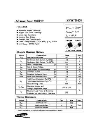
Advanced Power MOSFET FEATURES BVDSS = -250 V Avalanche Rugged Technology RDS(on) = 4.0 Rugged Gate Oxide Technology Lower Input Capacitance ID = -1.6 A Improved Gate Charge Extended Safe Operating Area Lower Leakage Current 10 A (Max.) @ VDS = -250V 2 Low RDS(ON) 3.5 (Typ.) 1 1 2 3 3 1. Gate 2. Drain 3. Source Absolute Maximum Ratings Symbol Char... See More ⇒
9.7. Size:502K samsung
sfw9634.pdf
Advanced Power MOSFET FEATURES BVDSS = -250 V Avalanche Rugged Technology RDS(on) = 1.3 Rugged Gate Oxide Technology Lower Input Capacitance ID = -5.0 A Improved Gate Charge Extended Safe Operating Area Lower Leakage Current 10 A (Max.) @ VDS = -250V 2 Low RDS(ON) 0.876 (Typ.) 1 1 2 3 3 1. Gate 2. Drain 3. Source Absolute Maximum Ratings Symbol Cha... See More ⇒
9.8. Size:506K samsung
sfw9640.pdf
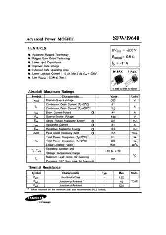
Advanced Power MOSFET FEATURES BVDSS = -200 V Avalanche Rugged Technology RDS(on) = 0.5 Rugged Gate Oxide Technology Lower Input Capacitance ID = -11 A Improved Gate Charge Extended Safe Operating Area Lower Leakage Current 10 A (Max.) @ VDS = -200V 2 Low RDS(ON) 0.344 (Typ.) 1 1 2 3 3 1. Gate 2. Drain 3. Source Absolute Maximum Ratings Symbol Cha... See More ⇒
9.9. Size:501K samsung
sfw9630.pdf

Advanced Power MOSFET FEATURES BVDSS = -200 V Avalanche Rugged Technology RDS(on) = 0.8 Rugged Gate Oxide Technology Lower Input Capacitance ID = -6.5 A Improved Gate Charge Extended Safe Operating Area Lower Leakage Current 10 A (Max.) @ VDS = -200V 2 Low RDS(ON) 0.581 (Typ.) 1 1 2 3 3 1. Gate 2. Drain 3. Source Absolute Maximum Ratings Symbol Ch... See More ⇒
9.10. Size:497K samsung
sfw9610.pdf

Advanced Power MOSFET FEATURES BVDSS = -200 V Avalanche Rugged Technology RDS(on) = 3.0 Rugged Gate Oxide Technology Lower Input Capacitance ID = -1.75 A Improved Gate Charge Extended Safe Operating Area Lower Leakage Current 10 A (Max.) @ VDS = -200V 2 Low RDS(ON) 2.084 (Typ.) 1 1 2 3 3 1. Gate 2. Drain 3. Source Absolute Maximum Ratings Symbol Ch... See More ⇒
Detailed specifications: SFW2955, SFW9510, SFW9520, SFW9530, SFW9540, SFW9610, SFW9614, SFW9620, AON7408, SFW9630, SFW9634, SFW9640, SFW9644, SFW9Z14, SFW9Z24, SFW9Z34, SI3443DVPBF
Keywords - SFW9624 MOSFET specs
SFW9624 cross reference
SFW9624 equivalent finder
SFW9624 pdf lookup
SFW9624 substitution
SFW9624 replacement
Need a MOSFET replacement?
Our guide shows you how to find a perfect substitute by comparing key parameters and specs
