2SK1143 Specs and Replacement
Type Designator: 2SK1143
Type of Transistor: MOSFET
Type of Control Channel: N-Channel
Absolute Maximum Ratings
Pd ⓘ - Maximum Power Dissipation: 35 W
|Vds|ⓘ - Maximum Drain-Source Voltage: 900 V
|Vgs|ⓘ - Maximum Gate-Source Voltage: 20 V
|Id| ⓘ - Maximum Drain Current: 2 A
Tj ⓘ - Maximum Junction Temperature: 150 °C
Electrical Characteristics
RDSonⓘ - Maximum Drain-Source On-State Resistance: 6 Ohm
Package: TO-220F
2SK1143 substitution
- MOSFET ⓘ Cross-Reference Search
2SK1143 datasheet
2sk1143.pdf
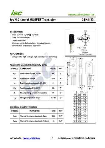
isc N-Channel MOSFET Transistor 2SK1143 DESCRIPTION Drain Current I =2A@ T =25 D C Drain Source Voltage- V =900V(Min) DSS Minimum Lot-to-Lot variations for robust device performance and reliable operation APPLICATIONS Designed for high voltage, high speed power switching ABSOLUTE MAXIMUM RATINGS(T =25 ) a SYMBOL ARAMETER VALUE UNIT V Drain-Source Voltage (V =0) 9... See More ⇒
2sk1142.pdf
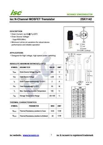
isc N-Channel MOSFET Transistor 2SK1142 DESCRIPTION Drain Current I =2A@ T =25 D C Drain Source Voltage- V =800V(Min) DSS Minimum Lot-to-Lot variations for robust device performance and reliable operation APPLICATIONS Designed for high voltage, high speed power switching ABSOLUTE MAXIMUM RATINGS(T =25 ) a SYMBOL ARAMETER VALUE UNIT V Drain-Source Voltage (V =0) 8... See More ⇒
2sk1188.pdf
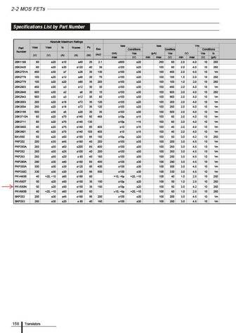
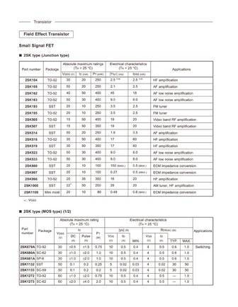
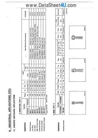
2-2 MOS FETs Specifications List by Part Number Absolute Maximum Ratings IGSS IDSS VTH VDSS VGSS ID ID (pulse) PD Part EAS Conditions Conditions Conditions Number (nA) VGS ( A) VDS (V) VDS ID (mJ) (V) (V) (A) (A) (W) max (V) min max (V) min max (V) ( A) 2SK1188 60 20 10 40 25 2.1 500 20 250 60 2.0 4.0 10 250 2SK2420 60 20 30 120 40 38 100 20 100 60 2.0 4.... See More ⇒
2sk1187.pdf
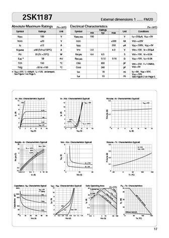
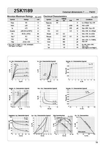
2SK1187 External dimensions 1 ...... FM20 Absolute Maximum Ratings Electrical Characteristics (Ta = 25 C) (Ta = 25 C) Ratings Symbol Ratings Unit Symbol Unit Conditions min typ max V 100 V V 100 V I = 250 A, V = 0V DSS (BR) DSS D GS V 20 V I 500 nA V = 20V GSS GSS GS I 12 A I 250 A V = 100V, V = 0V D DSS DS GS I V 2.0 4.0 V V = 10V, I = 250 A D (pulse) 48 (Tch 15... See More ⇒
2sk1179 2sk1183.pdf
2-2 MOS FETs Specifications List by Part Number Absolute Maximum Ratings IGSS IDSS VTH VDSS VGSS ID ID (pulse) PD Part EAS Conditions Conditions Conditions Number (nA) VGS ( A) VDS (V) VDS ID (mJ) (V) (V) (A) (A) (W) max (V) min max (V) min max (V) ( A) 2SK1179 500 20 8.5 34 85 400 500 20 250 500 2.0 4.0 10 250 2SK1183 200 20 3 12 25 30 500 20 250 200 2.0... See More ⇒
2sk1192.pdf
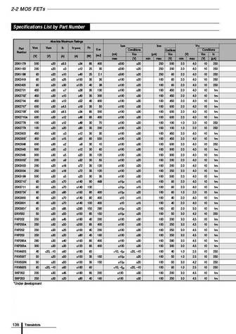
2SK1192 External dimensions 2 ...... FM100 Absolute Maximum Ratings Electrical Characteristics (Ta = 25 C) (Ta = 25 C) Ratings Symbol Ratings Unit Symbol Unit Conditions min typ max V 60 V V 60 V I = 250 A, V = 0V DSS (BR) DSS D GS V 20 V I 500 nA V = 20V GSS GSS GS I 40 A I 250 A V = 60V, V = 0V D DSS DS GS I 160 (Tch 150 C) A V 2.0 4.0 V V = 10V, I = 250 A D ... See More ⇒
2sk1178.pdf
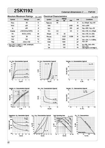
2SK1178 External dimensions 1 ...... FM20 Absolute Maximum Ratings Electrical Characteristics (Ta = 25 C) (Ta = 25 C) Ratings Symbol Ratings Unit Symbol Unit Conditions min typ max V 500 V V 500 V I = 250 A, V = 0V DSS (BR) DSS D GS V 20 V I 500 nA V = 20V GSS GSS GS I 4.0 A I 250 A V = 500V, V = 0V D DSS DS GS I 16 (Tch 150 C) A V 2.0 4.0 V V = 10V, I = 250 A D... See More ⇒
2sk1186.pdf

2SK1186 External dimensions 1 ...... FM20 Absolute Maximum Ratings Electrical Characteristics (Ta = 25 C) (Ta = 25 C) Ratings Symbol Ratings Unit Symbol Unit Conditions min typ max V 100 V V 100 V I = 250 A, V = 0V DSS (BR) DSS D GS V 20 V I 500 nA V = 20V GSS GSS GS I 9I 250 A V = 100V, V = 0V D A DSS DS GS I V 2.0 4.0 V V = 10V, I = 250 A D (pulse) 36 (Tch 150... See More ⇒
2sk1177.pdf
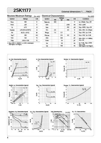
2SK1177 External dimensions 1......FM20 Absolute Maximum Ratings Electrical Characteristics (Ta = 25 C) (Ta = 25 C) Ratings Symbol Ratings Unit Symbol Unit Conditions min typ max V 500 V V 500 V I = 250 A, V = 0V DSS (BR) DSS D GS V 20 V I 500 nA V = 20V GSS GSS GS I 2.5 A I 250 A V = 500V, V = 0V D DSS DS GS I 10 (Tch 150 C) A V 2.0 4.0 V V = 10V, I = 250 A D (... See More ⇒
2sk104 2sk105 2sk162 2sk163 2sk193 2sk195 2sk505 2sk507 2sk514 2sk518 2sk519 2sk523 2sk533 2sk660 2sk997 2sk998 2sk1000 2sk1109.pdf
... See More ⇒
2sk1159 2sk1160.pdf
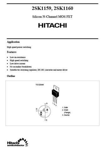
2SK1159, 2SK1160 Silicon N-Channel MOS FET Application High speed power switching Features Low on-resistance High speed switching Low drive current No secondary breakdown Suitable for switching regulator, DC-DC converter and motor driver Outline TO-220AB 1 D 2 3 1. Gate G 2. Drain (Flange) 3. Source S 2SK1159, 2SK1160 Absolute Maximum Ratings (Ta = 25... See More ⇒
2sk1184.pdf
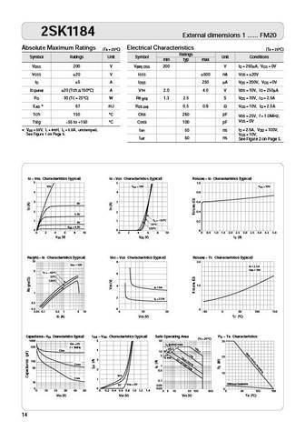
2SK1184 External dimensions 1 ...... FM20 Absolute Maximum Ratings Electrical Characteristics (Ta = 25 C) (Ta = 25 C) Ratings Symbol Ratings Unit Symbol Unit Conditions min typ max V 200 V V 200 V I = 250 A, V = 0V DSS (BR) DSS D GS V 20 V I 500 nA V = 20V GSS GSS GS I 5I 250 A V = 200V, V = 0V D A DSS DS GS I 20 (Tch 150 C) A V 2.0 4.0 V V = 10V, I = 250 A D (p... See More ⇒
2sk1180.pdf
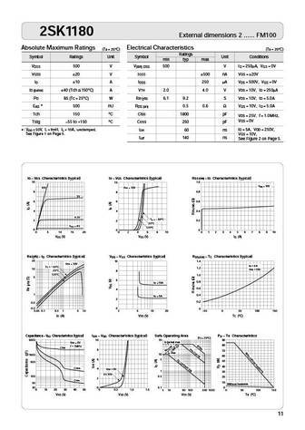
2SK1180 External dimensions 2 ...... FM100 Absolute Maximum Ratings Electrical Characteristics (Ta = 25 C) (Ta = 25 C) Ratings Symbol Ratings Unit Symbol Unit Conditions min typ max V 500 V V 500 V I = 250 A, V = 0V DSS (BR) DSS D GS V 20 V I 500 nA V = 20V GSS GSS GS I 10 A I 250 A V = 500V, V = 0V D DSS DS GS I 40 (Tch 150 C) A V 2.0 4.0 V V = 10V, I = 250 A D... See More ⇒
2sk118.pdf
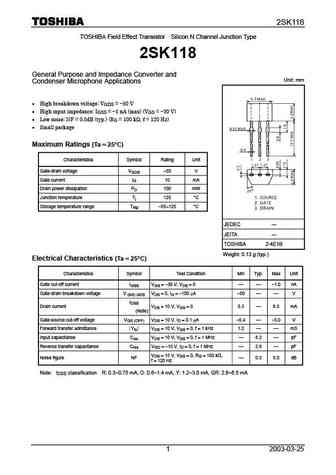
2SK118 TOSHIBA Field Effect Transistor Silicon N Channel Junction Type 2SK118 General Purpose and Impedance Converter and Unit mm Condenser Microphone Applications High breakdown voltage VGDS = -50 V High input impedance I = -1 nA (max) (V = -30 V) GSS GS Low noise NF = 0.5dB (typ.) (R = 100 k , f = 120 Hz) G Small package Maximum Ratings (Ta = = 25... See More ⇒
2sk117.pdf
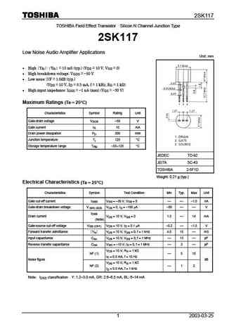
2SK117 TOSHIBA Field Effect Transistor Silicon N Channel Junction Type 2SK117 Low Noise Audio Amplifier Applications Unit mm High Yfs Y = 15 mS (typ.) (V = 10 V, V = 0) fs DS GS High breakdown voltage V = -50 V GDS Low noise NF = 1.0dB (typ.) (V = 10 V, I = 0.5 mA, f = 1 kHz, R = 1 k ) DS D G High input impedance I = -1 nA (max) (V = -30 V) GS... See More ⇒
2sk1120.pdf
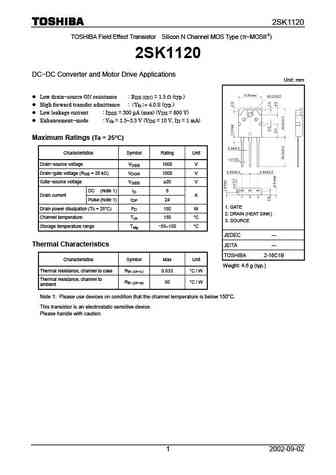
2SK1120 TOSHIBA Field Effect Transistor Silicon N Channel MOS Type ( -MOSII.5) 2SK1120 DC-DC Converter and Motor Drive Applications Unit mm Low drain-source ON resistance RDS (ON) = 1.5 (typ.) High forward transfer admittance Y 4.0 S (typ.) fs = Low leakage current I = 300 A (max) (V = 800 V) DSS DS Enhancement-mode Vth = 1.5 3.5 V (V = 10 V, I = 1 ... See More ⇒
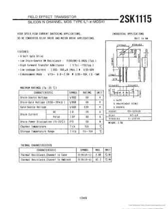
2sk1115.pdf
Free Datasheet http //www.datasheet4u.com/ Free Datasheet http //www.datasheet4u.com/ ... See More ⇒
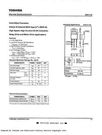
2sk1112.pdf
Powered by ICminer.com Electronic-Library Service CopyRight 2003 Powered by ICminer.com Electronic-Library Service CopyRight 2003 Powered by ICminer.com Electronic-Library Service CopyRight 2003 Powered by ICminer.com Electronic-Library Service CopyRight 2003 Powered by ICminer.com Electronic-Library Service CopyRight 2003 ... See More ⇒
2sk1119.pdf
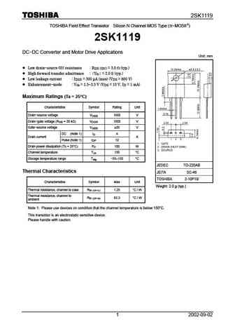
2SK1119 TOSHIBA Field Effect Transistor Silicon N Channel MOS Type ( -MOSII.5) 2SK1119 DC-DC Converter and Motor Drive Applications Unit mm Low drain-source ON resistance RDS (ON) = 3.0 (typ.) High forward transfer admittance Y = 2.0 S (typ.) fs Low leakage current I = 300 A (max) (V = 800 V) DSS DS Enhancement-mode Vth = 1.5 3.5 V (V = 10 V, I = 1 ... See More ⇒
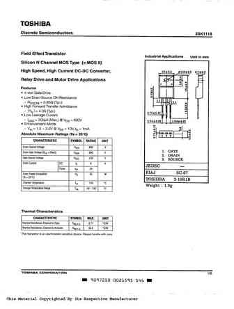
2sk1118.pdf
This Material Copyrighted By Its Respective Manufacturer This Material Copyrighted By Its Respective Manufacturer This Material Copyrighted By Its Respective Manufacturer This Material Copyrighted By Its Respective Manufacturer This Material Copyrighted By Its Respective Manufacturer ... See More ⇒
2sk1167.pdf

2SK1167, 2SK1168 Silicon N Channel MOS FET REJ03G0915-0200 (Previous ADE-208-1253) Rev.2.00 Sep 07, 2005 Application High speed power switching Features Low on-resistance High speed switching Low drive current No secondary breakdown Suitable for switching regulator and DC-DC converter Outline RENESAS Package code PRSS0004ZE-A (Package name T... See More ⇒
rej03g0910 2sk1157ds.pdf

To our customers, Old Company Name in Catalogs and Other Documents On April 1st, 2010, NEC Electronics Corporation merged with Renesas Technology Corporation, and Renesas Electronics Corporation took over all the business of both companies. Therefore, although the old company name remains in this document, it is a valid Renesas Electronics document. We appreciate your understanding. ... See More ⇒
2sk1153.pdf
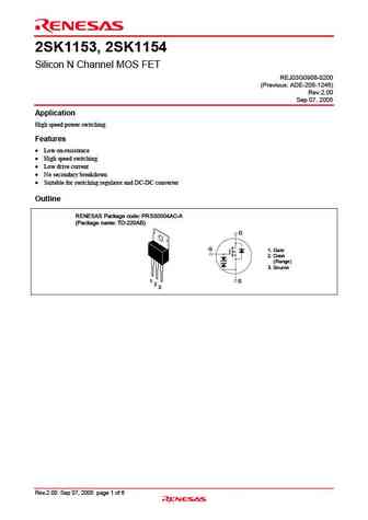
2SK1153, 2SK1154 Silicon N Channel MOS FET REJ03G0908-0200 (Previous ADE-208-1246) Rev.2.00 Sep 07, 2005 Application High speed power switching Features Low on-resistance High speed switching Low drive current No secondary breakdown Suitable for switching regulator and DC-DC converter Outline RENESAS Package code PRSS0004AC-A (Package name T... See More ⇒
2sk1161.pdf
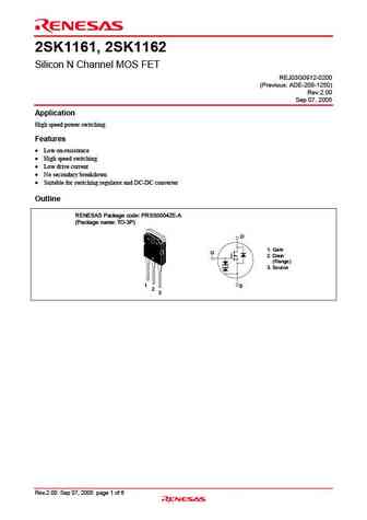
2SK1161, 2SK1162 Silicon N Channel MOS FET REJ03G0912-0200 (Previous ADE-208-1250) Rev.2.00 Sep 07, 2005 Application High speed power switching Features Low on-resistance High speed switching Low drive current No secondary breakdown Suitable for switching regulator and DC-DC converter Outline RENESAS Package code PRSS0004ZE-A (Package name T... See More ⇒
rej03g0916 2sk1169ds.pdf

To our customers, Old Company Name in Catalogs and Other Documents On April 1st, 2010, NEC Electronics Corporation merged with Renesas Technology Corporation, and Renesas Electronics Corporation took over all the business of both companies. Therefore, although the old company name remains in this document, it is a valid Renesas Electronics document. We appreciate your understanding. ... See More ⇒
2sk1155.pdf

2SK1155, 2SK1156 Silicon N Channel MOS FET REJ03G0909-0200 (Previous ADE-208-1247) Rev.2.00 Sep 07, 2005 Application High speed power switching Features Low on-resistance High speed switching Low drive current No secondary breakdown Suitable for switching regulator and DC-DC converter Outline RENESAS Package code PRSS0004AC-A (Package name T... See More ⇒
rej03g0911 2sk1159ds.pdf

To our customers, Old Company Name in Catalogs and Other Documents On April 1st, 2010, NEC Electronics Corporation merged with Renesas Technology Corporation, and Renesas Electronics Corporation took over all the business of both companies. Therefore, although the old company name remains in this document, it is a valid Renesas Electronics document. We appreciate your understanding. ... See More ⇒
2sk1151.pdf
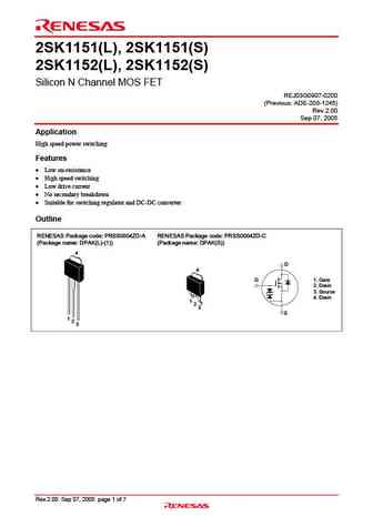
2SK1151(L), 2SK1151(S) 2SK1152(L), 2SK1152(S) Silicon N Channel MOS FET REJ03G0907-0200 (Previous ADE-208-1245) Rev.2.00 Sep 07, 2005 Application High speed power switching Features Low on-resistance High speed switching Low drive current No secondary breakdown Suitable for switching regulator and DC-DC converter Outline RENESAS Package code ... See More ⇒
2sk1163 2sk1164.pdf
To our customers, Old Company Name in Catalogs and Other Documents On April 1st, 2010, NEC Electronics Corporation merged with Renesas Technology Corporation, and Renesas Electronics Corporation took over all the business of both companies. Therefore, although the old company name remains in this document, it is a valid Renesas Electronics document. We appreciate your understanding. ... See More ⇒
2sk1165.pdf

2SK1165, 2SK1166 Silicon N Channel MOS FET REJ03G0914-0200 (Previous ADE-208-1252) Rev.2.00 Sep 07, 2005 Application High speed power switching Features Low on-resistance High speed switching Low drive current No secondary breakdown Suitable for switching regulator and DC-DC converter Outline RENESAS Package code PRSS0004ZE-A (Package name T... See More ⇒
rej03g0912 2sk1161ds.pdf

To our customers, Old Company Name in Catalogs and Other Documents On April 1st, 2010, NEC Electronics Corporation merged with Renesas Technology Corporation, and Renesas Electronics Corporation took over all the business of both companies. Therefore, although the old company name remains in this document, it is a valid Renesas Electronics document. We appreciate your understanding. ... See More ⇒
2sk1159 2sk1160.pdf
2SK1159, 2SK1160 Silicon N Channel MOS FET REJ03G0911-0200 (Previous ADE-208-1249) Rev.2.00 Sep 07, 2005 Application High speed power switching Features Low on-resistance High speed switching Low drive current No secondary breakdown Suitable for switching regulator, DC-DC converter and motor driver Outline RENESAS Package code PRSS0004AC-A ... See More ⇒
rej03g0915 2sk1167ds.pdf

To our customers, Old Company Name in Catalogs and Other Documents On April 1st, 2010, NEC Electronics Corporation merged with Renesas Technology Corporation, and Renesas Electronics Corporation took over all the business of both companies. Therefore, although the old company name remains in this document, it is a valid Renesas Electronics document. We appreciate your understanding. ... See More ⇒
2sk1157.pdf
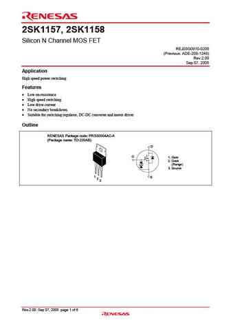
2SK1157, 2SK1158 Silicon N Channel MOS FET REJ03G0910-0200 (Previous ADE-208-1248) Rev.2.00 Sep 07, 2005 Application High speed power switching Features Low on-resistance High speed switching Low drive current No secondary breakdown Suitable for switching regulator, DC-DC converter and motor driver Outline RENESAS Package code PRSS0004AC-A (P... See More ⇒
rej03g0909 2sk1155ds.pdf
To our customers, Old Company Name in Catalogs and Other Documents On April 1st, 2010, NEC Electronics Corporation merged with Renesas Technology Corporation, and Renesas Electronics Corporation took over all the business of both companies. Therefore, although the old company name remains in this document, it is a valid Renesas Electronics document. We appreciate your understanding. ... See More ⇒
r07ds0397ej 2sk115152.pdf
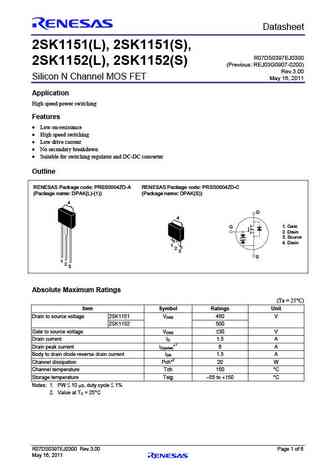
Preliminary Datasheet 2SK1151(L), 2SK1151(S), R07DS0397EJ0300 2SK1152(L), 2SK1152(S) (Previous REJ03G0907-0200) Rev.3.00 Silicon N Channel MOS FET May 16, 2011 Application High speed power switching Features Low on-resistance High speed switching Low drive current No secondary breakdown Suitable for switching regulator and DC-DC converter Outlin... See More ⇒
2sk1108.pdf
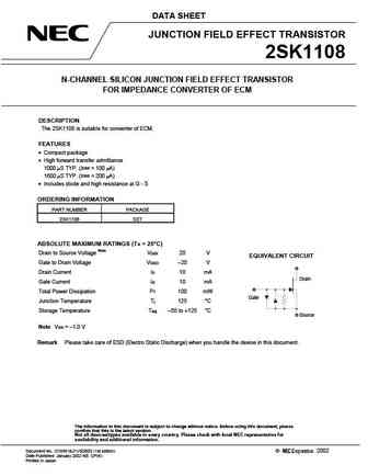
DATA SHEET JUNCTION FIELD EFFECT TRANSISTOR 2SK1108 N-CHANNEL SILICON JUNCTION FIELD EFFECT TRANSISTOR FOR IMPEDANCE CONVERTER OF ECM DESCRIPTION The 2SK1108 is suitable for converter of ECM. FEATURES Compact package High forward transfer admittance 1000 S TYP. (IDSS = 100 A) 1600 S TYP. (IDSS = 200 A) Includes diode and high resistance at G - S ORDERING INFORM... See More ⇒
2sk1109.pdf
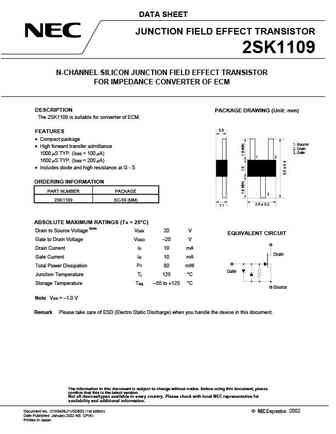
DATA SHEET JUNCTION FIELD EFFECT TRANSISTOR 2SK1109 N-CHANNEL SILICON JUNCTION FIELD EFFECT TRANSISTOR FOR IMPEDANCE CONVERTER OF ECM DESCRIPTION PACKAGE DRAWING (Unit mm) The 2SK1109 is suitable for converter of ECM. 0.8 FEATURES Compact package 1. Source High forward transfer admittance 2. Drain 3. Gate 1000 S TYP. (IDSS = 100 A) 1 2 1600 S TYP. (IDSS = 200 ... See More ⇒
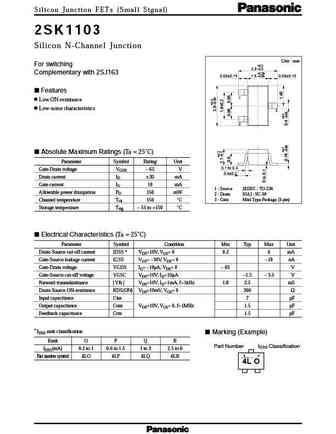
2sk1103.pdf
Silicon Junction FETs (Small Signal) 2SK1103 2SK1103 Silicon N-Channel Junction Unit mm For switching +0.2 2.8 0.3 Complementary with 2SJ163 +0.25 0.65 0.15 1.5 0.05 0.65 0.15 Features 1 Low ON-resistance Low-noise characteristics 3 2 Absolute Maximum Ratings (Ta = 25 C) Parameter Symbol Rating Unit 0.1 to 0.3 Gate-Drain voltage VGDS 65 V 0.4 0.2 Drain c... See More ⇒
2sk1104.pdf
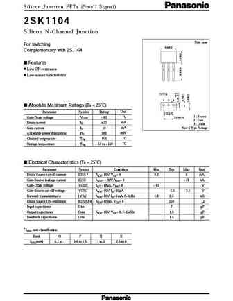
Silicon Junction FETs (Small Signal) 2SK1104 2SK1104 Silicon N-Channel Junction Unit mm For switching 4.0 0.2 Complementary with 2SJ164 Features Low ON-resistance Low-noise characteristics marking 1 2 3 Absolute Maximum Ratings (Ta = 25 C) Parameter Symbol Rating Unit 1.27 1.27 1 Source Gate-Drain voltage VGDS 65 V 2.54 0.15 2 Gate Drain current ID 20 mA 3 ... See More ⇒
2sk1109.pdf
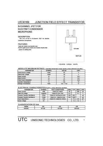
UTC K1109 JUNCTION FIELD EFFECT TRANSISTOR N-CHANNEL JFET FOR ELECTRET CONDENSER MICROPHONE 1 2 DESCRIPTION The UTC K1109 is N-channel JFET for electret condenser microphone. 3 FEATURES *High gm implies low transfer loss *Built-in gate-source diode and resistor implies fast TOP VIEW power on settling time SOT-23 1 SOURCE 2 DRAIN 3 GATE ABSOLUTE MAXIMUM RATINGS ( Operating tem... See More ⇒
2sk1197.pdf
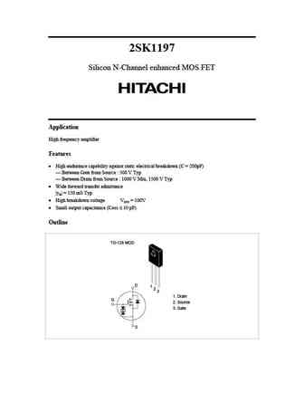
2SK1197 Silicon N-Channel enhanced MOS FET Application High frequency amplifier Features High endurance capability against static electrical breakdown (C = 200pF) Between Gate from Source 500 V Typ Between Drain from Source 1000 V Min, 1500 V Typ Wide forward transfer admittance yfs = 150 mS Typ High breakdown voltage VDSS = 100V Small output capacitance... See More ⇒
2sk1169 2sk1170.pdf
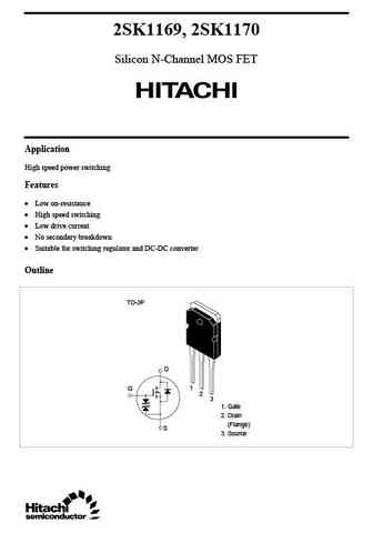
2SK1169, 2SK1170 Silicon N-Channel MOS FET Application High speed power switching Features Low on-resistance High speed switching Low drive current No secondary breakdown Suitable for switching regulator and DC-DC converter Outline TO-3P D 1 G 2 3 1. Gate 2. Drain (Flange) S 3. Source 2SK1169, 2SK1170 Absolute Maximum Ratings (Ta = 25 C) Item Symbol... See More ⇒
2sk1185.pdf
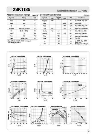
2SK1185 External dimensions 1 ...... FM20 Absolute Maximum Ratings Electrical Characteristics (Ta = 25 C) (Ta = 25 C) Ratings Symbol Ratings Unit Symbol Unit Conditions min typ max V 100 V V 100 V I = 250 A, V = 0V DSS (BR) DSS D GS V 20 V I 500 nA V = 20V GSS GSS GS I 5I 250 A V = 100V, V = 0V D A DSS DS GS I 20 (Tch 150 C) A V 2.0 4.0 V V = 10V, I = 250 A D (... See More ⇒
2sk1191.pdf

2SK1191 External dimensions 1 ...... FM20 Absolute Maximum Ratings Electrical Characteristics (Ta = 25 C) (Ta = 25 C) Ratings Symbol Ratings Unit Symbol Unit Conditions min typ max V 60 V V 60 V I = 250 A, V = 0V DSS (BR) DSS D GS V 20 V I 500 nA V = 20V GSS GSS GS I 30 A I 250 A V = 60V, V = 0V D DSS DS GS I 120 (Tch 150 C) A V 2.0 4.0 V V = 10V, I = 250 A D (p... See More ⇒
2sk1190.pdf
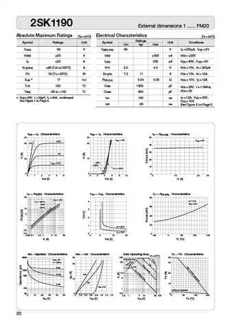
2SK1190 External dimensions 1 ...... FM20 Absolute Maximum Ratings Electrical Characteristics (Ta = 25 C) (Ta = 25 C) Ratings Symbol Ratings Unit Symbol Unit Conditions min typ max V 60 V V 60 V I = 250 A, V = 0V DSS (BR) DSS D GS V 20 V I 500 nA V = 20V GSS GSS GS I 22 A I 250 A V = 60V, V = 0V D DSS DS GS I 88 (Tch 150 C) A V 2.0 4.0 V V = 10V, I = 250 A D (pu... See More ⇒
2sk1181.pdf
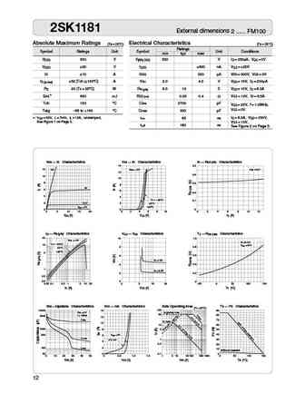
2SK1181 External dimensions 2 ...... FM100 Absolute Maximum Ratings Electrical Characteristics (Ta = 25 C) (Ta = 25 C) Ratings Symbol Ratings Unit Symbol Unit Conditions min typ max V 500 V V 500 V I = 250 A, V = 0V DSS (BR) DSS D GS V 20 V I 500 nA V = 20V GSS GSS GS I 13 A I 250 A V = 500V, V = 0V D DSS DS GS I 52 (Tch 150 C) A V 2.0 4.0 V V = 10V, I = 250 A ... See More ⇒
2sk113 2sk152 2sk363 2sj44 ifn113 ifn152 ifn363 ifp44.pdf
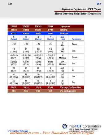
Databook.fxp 1/13/99 2 09 PM Page D-3 01/99 D-3 Japanese Equivalent JFET Types Silicon Junction Field-Effect Transistors 2SK113 2SK152 2SK363 2SJ44 Japanese IFN113 IFN152 IFN363 IFP44 InterFET NJ132 NJ132L NJ450 PJ99 Process N N N P Unit Channel Channel Channel Channel Limit Parameters V 50 20 40 25 BVGSS Min 1.0 0.1 1.0 1.0 nA IGSS ( 20 V) ( 10 V) ( 30 V) (... See More ⇒
2sk1109.pdf
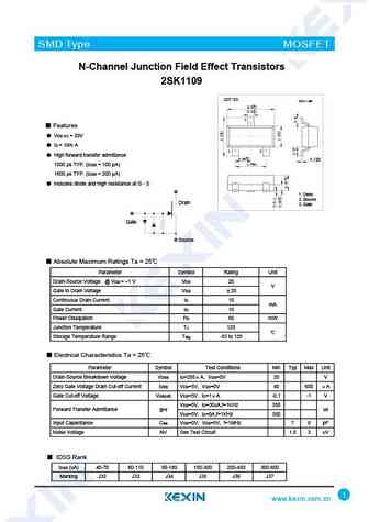
SMD Type MOSFET N-Channel Junction Field Effect Transistors 2SK1109 SOT-23 Unit mm +0.1 2.9 -0.1 +0.1 0.4 -0.1 3 Features VDS (V) = 20V ID = 10m A 1 2 High forward transfer admittance +0.1 +0.05 0.95 -0.1 0.1 -0.01 +0.1 1.9-0.1 1000 s TYP. (IDSS = 100 A) 1600 s TYP. (IDSS = 200 A) Includes diode and high resistance at G - S 1. Drain 2. So... See More ⇒
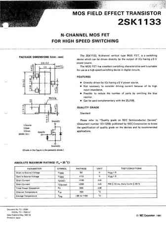
2sk1133.pdf
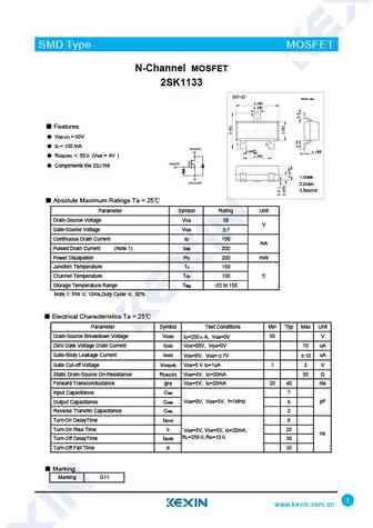
SMD Type MOSFET N-Channel MOSFET 2SK1133 SOT-23 Unit mm +0.1 2.9 -0.1 +0.1 0.4 -0.1 3 Features VDS (V) = 50V 1 2 ID = 100 mA +0.1 +0.05 0.95-0.1 0.1-0.01 +0.1 1.9-0.1 RDS(ON) 50 (VGS = 4V ) Complments the 2SJ166 1.Gate 2.Drain 3.Source Absolute Maximum Ratings Ta = 25 Parameter Symbol Rating Unit Drain-Source Voltage VDS 50 V G... See More ⇒
2sk1133-3.pdf
SMD Type MOSFET N-Channel MOSFET 2SK1133 SOT-23-3 Unit mm +0.2 2.9-0.1 +0.1 0.4 -0.1 3 Features VDS (V) = 50V 1 2 ID = 100 mA +0.02 +0.1 0.15 -0.02 0.95 -0.1 RDS(ON) 50 (VGS = 4V ) +0.1 1.9 -0.2 Complments the 2SJ166 1. Gate 2. Source 3. Drain Absolute Maximum Ratings Ta = 25 Parameter Symbol Rating Unit Drain-Source Voltage VDS 5... See More ⇒
2sk1167.pdf
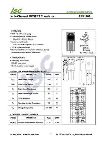
isc N-Channel MOSFET Transistor 2SK1167 FEATURES With TO-3PN packaging Low drain-source on-resistance RDS(ON) =0.36 (MAX) Enhancement mode Vth = 3.0 to 4.0V (VDS = 10 V, ID=1mA) 100% avalanche tested Minimum Lot-to-Lot variations for robust device performance and reliable operationz APPLICATIONS Switching applications DC-DC converters Uninterruptible power ... See More ⇒
2sk1158.pdf

isc N-Channel MOSFET Transistor 2SK1158 FEATURES Drain Current I = 7.0A@ T =25 D C Drain Source Voltage- V = 500V(Min) DSS Static Drain-Source On-Resistance R = 0.9 (Max) DS(on) 100% avalanche tested Minimum Lot-to-Lot variations for robust device performance and reliable operation DESCRIPTION Designed for use in switch mode power supplies and general purpo... See More ⇒
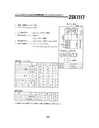
2sk1117.pdf

isc N-Channel MOSFET Transistor 2SK1117 FEATURES Drain Current I = 6.0A@ T =25 D C Drain Source Voltage- V =600V(Min) DSS Static Drain-Source On-Resistance R = 1.25 (Max) DS(on) 100% avalanche tested Minimum Lot-to-Lot variations for robust device performance and reliable operation DESCRIPTION Designed for use in switch mode power supplies and general purpo... See More ⇒
2sk1120.pdf

isc N-Channel MOSFET Transistor 2SK1120 FEATURES Drain Current I = 8.0A@ T =25 D C Drain Source Voltage- V = 1000V(Min) DSS Static Drain-Source On-Resistance R = 1.8 (Max) DS(on) 100% avalanche tested Minimum Lot-to-Lot variations for robust device performance and reliable operation DESCRIPTION Designed for use in switch mode power supplies and general purp... See More ⇒
2sk1160.pdf

isc N-Channel MOSFET Transistor 2SK1160 FEATURES Drain Current I = 8.0A@ T =25 D C Drain Source Voltage- V = 500V(Min) DSS Static Drain-Source On-Resistance R = 0.8 (Max) DS(on) 100% avalanche tested Minimum Lot-to-Lot variations for robust device performance and reliable operation DESCRIPTION Designed for use in switch mode power supplies and general purpo... See More ⇒
2sk1162.pdf
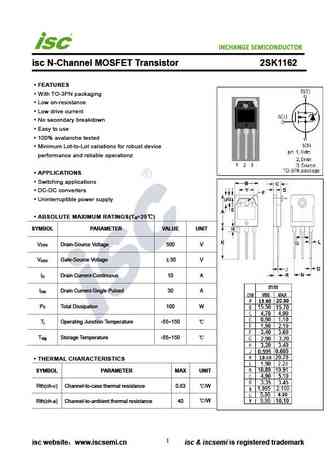
INCHANGE Semiconductor isc N-Channel MOSFET Transistor 2SK1162 FEATURES With TO-3PN packaging Low on-resistance Low drive current No secondary breakdown Easy to use 100% avalanche tested Minimum Lot-to-Lot variations for robust device performance and reliable operationz APPLICATIONS Switching applications DC-DC converters Uninterruptible power supply ABS... See More ⇒
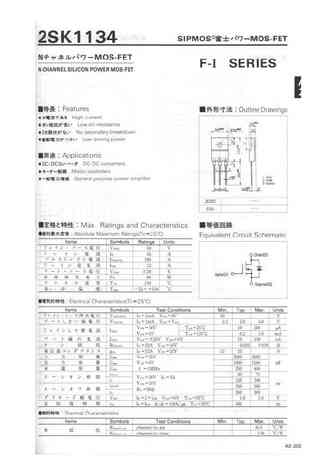
2sk1134.pdf
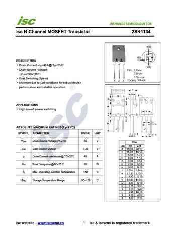
isc N-Channel MOSFET Transistor 2SK1134 DESCRIPTION Drain Current I =45A@ T =25 D C Drain Source Voltage- V =50V(Min) DSS Fast Switching Speed Minimum Lot-to-Lot variations for robust device performance and reliable operation APPLICATIONS High speed power switching ABSOLUTE MAXIMUM RATINGS(T =25 ) a SYMBOL ARAMETER VALUE UNIT V Drain-Source Voltage (V =0) 50 V... See More ⇒
2sk1115.pdf

isc N-Channel MOSFET Transistor 2SK1115 FEATURES Drain Current I = 20A@ T =25 D C Drain Source Voltage- V =60V(Min) DSS Static Drain-Source On-Resistance R = 55m (Max) DS(on) 100% avalanche tested Minimum Lot-to-Lot variations for robust device performance and reliable operation DESCRIPTION Designed for use in switch mode power supplies and general purpose ... See More ⇒
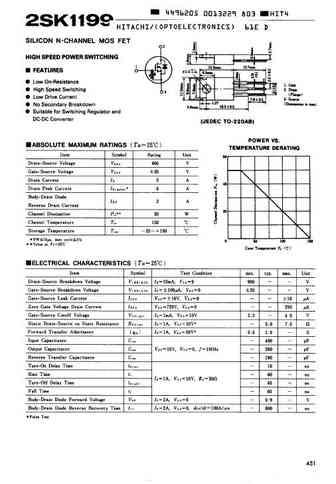
2sk1199.pdf
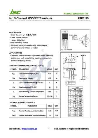
isc N-Channel MOSFET Transistor 2SK1199 DESCRIPTION Drain Current I = 2A@ T =25 D C Drain Source Voltage- V = 900V(Min) DSS Fast Switching Speed Minimum Lot-to-Lot variations for robust device performance and reliable operation APPLICATIONS Designed for high voltage, high speed power switching applications such as switching regulators, converters, solenoid and rel... See More ⇒
2sk1170.pdf

isc N-Channel MOSFET Transistor 2SK1170 FEATURES Drain Current I = 20A@ T =25 D C Drain Source Voltage- V = 500V(Min) DSS Static Drain-Source On-Resistance R = 0.27 (Max) DS(on) 100% avalanche tested Minimum Lot-to-Lot variations for robust device performance and reliable operation DESCRIPTION Designed for use in switch mode power supplies and general purpo... See More ⇒
2sk1114.pdf
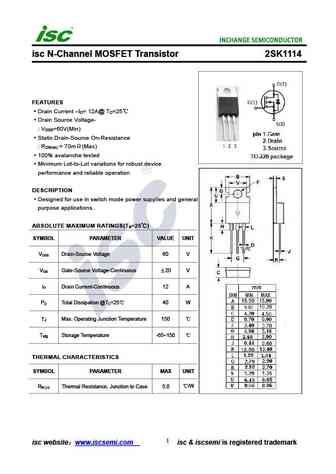
isc N-Channel MOSFET Transistor 2SK1114 FEATURES Drain Current I = 12A@ T =25 D C Drain Source Voltage- V =60V(Min) DSS Static Drain-Source On-Resistance R = 70m (Max) DS(on) 100% avalanche tested Minimum Lot-to-Lot variations for robust device performance and reliable operation DESCRIPTION Designed for use in switch mode power supplies and general purpose ... See More ⇒
2sk1151l.pdf

isc N-Channel MOSFET Transistor 2SK1151L FEATURES Drain Current I = 1.5A@ T =25 D C Drain Source Voltage- V = 450V(Min) DSS Static Drain-Source On-Resistance R = 5.5 (Max) DS(on) 100% avalanche tested Minimum Lot-to-Lot variations for robust device performance and reliable operation DESCRIPTION Designed for use in switch mode power supplies and general purp... See More ⇒
2sk1153.pdf

isc N-Channel MOSFET Transistor 2SK1153 FEATURES Drain Current I = 3.0A@ T =25 D C Drain Source Voltage- V = 450V(Min) DSS Static Drain-Source On-Resistance R = 2.8 (Max) DS(on) 100% avalanche tested Minimum Lot-to-Lot variations for robust device performance and reliable operation DESCRIPTION Designed for use in switch mode power supplies and general purpo... See More ⇒
2sk1116.pdf

isc N-Channel MOSFET Transistor 2SK1116 FEATURES Drain Current I = 25A@ T =25 D C Drain Source Voltage- V =100V(Min) DSS Static Drain-Source On-Resistance R = 58m (Max) DS(on) 100% avalanche tested Minimum Lot-to-Lot variations for robust device performance and reliable operation DESCRIPTION Designed for use in switch mode power supplies and general purpose... See More ⇒
2sk1161.pdf

isc N-Channel MOSFET Transistor 2SK1161 FEATURES Drain Current I = 10A@ T =25 D C Drain Source Voltage- V = 450V(Min) DSS Static Drain-Source On-Resistance R = 0.8 (Max) DS(on) 100% avalanche tested Minimum Lot-to-Lot variations for robust device performance and reliable operation DESCRIPTION Designed for use in switch mode power supplies and general purpos... See More ⇒
2sk1152l.pdf
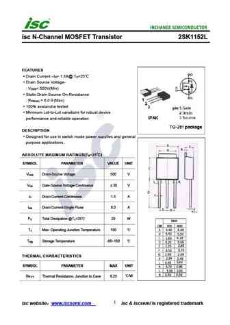
isc N-Channel MOSFET Transistor 2SK1152L FEATURES Drain Current I = 1.5A@ T =25 D C Drain Source Voltage- V = 500V(Min) DSS Static Drain-Source On-Resistance R = 6.0 (Max) DS(on) 100% avalanche tested Minimum Lot-to-Lot variations for robust device performance and reliable operation DESCRIPTION Designed for use in switch mode power supplies and general purp... See More ⇒
2sk1155.pdf

isc N-Channel MOSFET Transistor 2SK1155 FEATURES Drain Current I = 5.0A@ T =25 D C Drain Source Voltage- V = 450V(Min) DSS Static Drain-Source On-Resistance R = 1.4 (Max) DS(on) 100% avalanche tested Minimum Lot-to-Lot variations for robust device performance and reliable operation DESCRIPTION Designed for use in switch mode power supplies and general purpo... See More ⇒
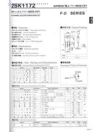
2sk1172.pdf
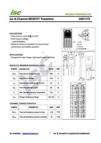
isc N-Channel MOSFET Transistor 2SK1172 DESCRIPTION Drain Current I =3.5A@ T =25 D C Drain Source Voltage- V =900V(Min) DSS Minimum Lot-to-Lot variations for robust device performance and reliable operation APPLICATIONS Designed for high voltage, high speed power switching ABSOLUTE MAXIMUM RATINGS(T =25 ) a SYMBOL ARAMETER VALUE UNIT V Drain-Source Voltage (V =0)... See More ⇒
2sk1169.pdf
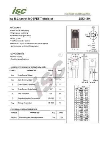
isc N-Channel MOSFET Transistor 2SK1169 FEATURES With TO-3P packaging High speed switching Standard level gate drive Easy to use 100% avalanche tested Minimum Lot-to-Lot variations for robust device performance and reliable operation APPLICATIONS Power supply Switching applications ABSOLUTE MAXIMUM RATINGS(T =25 ) a SYMBOL PARAMETER VALUE UNIT V Drain-Sour... See More ⇒
2sk1152s.pdf

isc N-Channel MOSFET Transistor 2SK1152S FEATURES Drain Current I = 1.5A@ T =25 D C Drain Source Voltage- V = 500V(Min) DSS Static Drain-Source On-Resistance R = 6.0 (Max) DS(on) 100% avalanche tested Minimum Lot-to-Lot variations for robust device performance and reliable operation DESCRIPTION Designed for use in switch mode power supplies and general purp... See More ⇒
2sk1154.pdf

isc N-Channel MOSFET Transistor 2SK1154 FEATURES Drain Current I = 3.0A@ T =25 D C Drain Source Voltage- V = 500V(Min) DSS Static Drain-Source On-Resistance R = 3.0 (Max) DS(on) 100% avalanche tested Minimum Lot-to-Lot variations for robust device performance and reliable operation DESCRIPTION Designed for use in switch mode power supplies and general purpo... See More ⇒
2sk1197.pdf
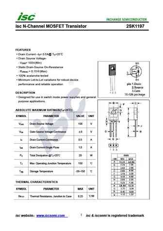
isc N-Channel MOSFET Transistor 2SK1197 FEATURES Drain Current I = 0.5A@ T =25 D C Drain Source Voltage- V = 100V(Min) DSS Static Drain-Source On-Resistance R = 0.15 (Max) DS(on) 100% avalanche tested Minimum Lot-to-Lot variations for robust device performance and reliable operation DESCRIPTION Designed for use in switch mode power supplies and general purp... See More ⇒
2sk1119.pdf

isc N-Channel MOSFET Transistor 2SK1119 FEATURES Drain Current I = 4.0A@ T =25 D C Drain Source Voltage- V = 1000V(Min) DSS Static Drain-Source On-Resistance R = 3.8 (Max) DS(on) 100% avalanche tested Minimum Lot-to-Lot variations for robust device performance and reliable operation DESCRIPTION Designed for use in switch mode power supplies and general purp... See More ⇒
2sk1151s.pdf
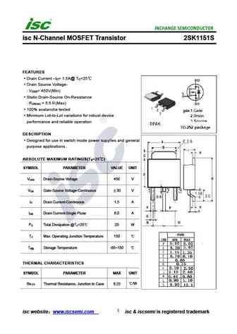
isc N-Channel MOSFET Transistor 2SK1151S FEATURES Drain Current I = 1.5A@ T =25 D C Drain Source Voltage- V = 450V(Min) DSS Static Drain-Source On-Resistance R = 5.5 (Max) DS(on) 100% avalanche tested Minimum Lot-to-Lot variations for robust device performance and reliable operation DESCRIPTION Designed for use in switch mode power supplies and general purp... See More ⇒
2sk1168.pdf

isc N-Channel MOSFET Transistor 2SK1168 FEATURES Drain Current I = 15A@ T =25 D C Drain Source Voltage- V = 500V(Min) DSS Static Drain-Source On-Resistance R = 0.4 (Max) DS(on) 100% avalanche tested Minimum Lot-to-Lot variations for robust device performance and reliable operation DESCRIPTION Designed for use in switch mode power supplies and general purpos... See More ⇒
2sk1165.pdf

isc N-Channel MOSFET Transistor 2SK1165 FEATURES Drain Current I = 12A@ T =25 D C Drain Source Voltage- V = 450V(Min) DSS Static Drain-Source On-Resistance R = 0.55 (Max) DS(on) 100% avalanche tested Minimum Lot-to-Lot variations for robust device performance and reliable operation DESCRIPTION Designed for use in switch mode power supplies and general purpo... See More ⇒
2sk1164.pdf

isc N-Channel MOSFET Transistor 2SK1164 FEATURES Drain Current I = 11A@ T =25 D C Drain Source Voltage- V = 450V(Min) DSS Static Drain-Source On-Resistance R = 0.7 (Max) DS(on) 100% avalanche tested Minimum Lot-to-Lot variations for robust device performance and reliable operation DESCRIPTION Designed for use in switch mode power supplies and general purpos... See More ⇒
2sk1166.pdf

isc N-Channel MOSFET Transistor 2SK1166 FEATURES Drain Current I = 12A@ T =25 D C Drain Source Voltage- V = 500V(Min) DSS Static Drain-Source On-Resistance R = 0.6 (Max) DS(on) 100% avalanche tested Minimum Lot-to-Lot variations for robust device performance and reliable operation DESCRIPTION Designed for use in switch mode power supplies and general purpos... See More ⇒
2sk1156.pdf
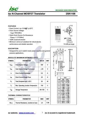
isc N-Channel MOSFET Transistor 2SK1156 FEATURES Drain Current I = 5.0A@ T =25 D C Drain Source Voltage- V = 500V(Min) DSS Static Drain-Source On-Resistance R = 1.5 (Max) DS(on) 100% avalanche tested Minimum Lot-to-Lot variations for robust device performance and reliable operation DESCRIPTION Designed for use in switch mode power supplies and general purpo... See More ⇒
2sk1118.pdf
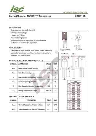
isc N-Channel MOSFET Transistor 2SK1118 DESCRIPTION Drain Current I =6A@ T =25 D C Drain Source Voltage- V = 600V(Min) DSS Fast Switching Speed Minimum Lot-to-Lot variations for robust device performance and reliable operation APPLICATIONS Designed for high voltage, high speed power switching applications such as switching regulators, converters, solenoid and rela... See More ⇒
2sk1171.pdf
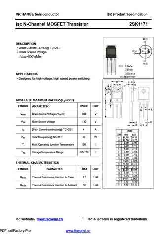
INCHANGE Semiconductor isc Product Specification isc N-Channel MOSFET Transistor 2SK1171 DESCRIPTION Drain Current ID=4A@ TC=25 Drain Source Voltage- VDSS=800V(Min) APPLICATIONS Designed for high voltage, high speed power switching ABSOLUTE MAXIMUM RATINGS(Ta=25 ) SYMBOL VALUE UNIT ARAMETER VDSS Drain-Source Voltage (VGS=0) 800 V VGS Gate-Source Voltage ... See More ⇒
2sk1163.pdf
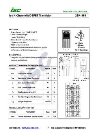
isc N-Channel MOSFET Transistor 2SK1163 FEATURES Drain Current I = 11A@ T =25 D C Drain Source Voltage- V = 450V(Min) DSS Static Drain-Source On-Resistance R = 0.7 (Max) DS(on) 100% avalanche tested Minimum Lot-to-Lot variations for robust device performance and reliable operation DESCRIPTION Designed for use in switch mode power supplies and general purpos... See More ⇒
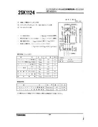
2sk1124.pdf
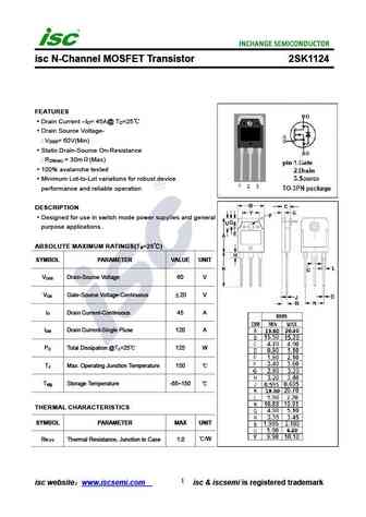
isc N-Channel MOSFET Transistor 2SK1124 FEATURES Drain Current I = 45A@ T =25 D C Drain Source Voltage- V = 60V(Min) DSS Static Drain-Source On-Resistance R = 30m (Max) DS(on) 100% avalanche tested Minimum Lot-to-Lot variations for robust device performance and reliable operation DESCRIPTION Designed for use in switch mode power supplies and general purpose... See More ⇒
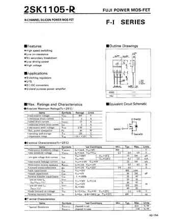
2sk1105.pdf
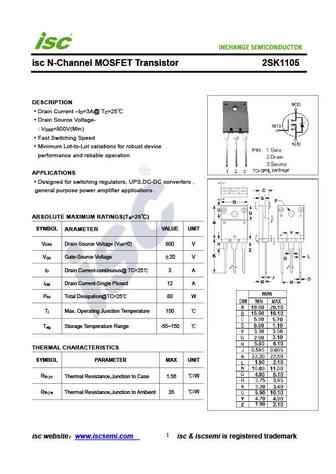
isc N-Channel MOSFET Transistor 2SK1105 DESCRIPTION Drain Current I =3A@ T =25 D C Drain Source Voltage- V =800V(Min) DSS Fast Switching Speed Minimum Lot-to-Lot variations for robust device performance and reliable operation APPLICATIONS Designed for switching regulators, UPS,DC-DC converters , general purpose power amplifier applications . ABSOLUTE MAXIMUM RATIN... See More ⇒
2sk1157.pdf

isc N-Channel MOSFET Transistor 2SK1157 FEATURES Drain Current I = 7.0A@ T =25 D C Drain Source Voltage- V = 450V(Min) DSS Static Drain-Source On-Resistance R = 0.8 (Max) DS(on) 100% avalanche tested Minimum Lot-to-Lot variations for robust device performance and reliable operation DESCRIPTION Designed for use in switch mode power supplies and general purpo... See More ⇒
2sk1180.pdf
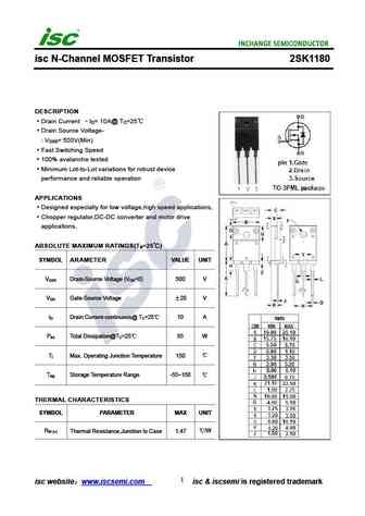
isc N-Channel MOSFET Transistor 2SK1180 DESCRIPTION Drain Current I = 10A@ T =25 D C Drain Source Voltage- V = 500V(Min) DSS Fast Switching Speed 100% avalanche tested Minimum Lot-to-Lot variations for robust device performance and reliable operation APPLICATIONS Designed especially for low voltage,high speed applications, Chopper regulator,DC-DC converter and... See More ⇒
2sk1159.pdf

isc N-Channel MOSFET Transistor 2SK1159 FEATURES Drain Current I = 8.0A@ T =25 D C Drain Source Voltage- V = 450V(Min) DSS Static Drain-Source On-Resistance R = 0.7 (Max) DS(on) 100% avalanche tested Minimum Lot-to-Lot variations for robust device performance and reliable operation DESCRIPTION Designed for use in switch mode power supplies and general purpo... See More ⇒
Detailed specifications: 2SK1013, 2SK1014, 2SK1023, 2SK1024, 2SK1073, 2SK1081, 2SK1134, 2SK1142, 2N60, 2SK1212, 2SK1319, 2SK1320, 2SK1324, 2SK1373, 2SK1385, 2SK1386, 2SK1401
Keywords - 2SK1143 MOSFET specs
2SK1143 cross reference
2SK1143 equivalent finder
2SK1143 pdf lookup
2SK1143 substitution
2SK1143 replacement
Can't find your MOSFET? Learn how to find a substitute transistor by analyzing voltage, current and package compatibility
🌐 : EN ES РУ

LIST
Last Update
MOSFET: AUB062N08BG | AUB060N08AG | AUB056N10 | AUB056N08BGL | AUB050N085 | AUB050N055 | AUB045N12 | AUB045N10BT | AUB039N10 | AUB034N10
Popular searches
m28s transistor | 2n3640 | tta1943 transistor | fb4410z | 2sa899 | 2sc1166 | jcs9n50fc datasheet | 2n2147