2SK2117 Specs and Replacement
Type Designator: 2SK2117
Type of Transistor: MOSFET
Type of Control Channel: N-Channel
Absolute Maximum Ratings
Pd ⓘ
- Maximum Power Dissipation: 35 W
|Vds|ⓘ - Maximum Drain-Source Voltage: 500 V
|Vgs|ⓘ - Maximum Gate-Source Voltage: 30 V
|Id| ⓘ - Maximum Drain Current: 7 A
Tj ⓘ - Maximum Junction Temperature: 150 °C
Electrical Characteristics
tr ⓘ - Rise Time: 55 nS
Cossⓘ -
Output Capacitance: 280 pF
RDSonⓘ - Maximum Drain-Source On-State Resistance: 0.9 Ohm
Package: TO-220F
- MOSFET ⓘ Cross-Reference Search
2SK2117 datasheet
..1. Size:32K hitachi
2sk2116 2sk2117.pdf 
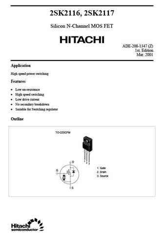
2SK2116, 2SK2117 Silicon N-Channel MOS FET ADE-208-1347 (Z) 1st. Edition Mar. 2001 Application High speed power switching Features Low on-resistance High speed switching Low drive current No secondary breakdown Suitable for Switching regulator Outline TO-220CFM 1 D 2 3 1. Gate G 2. Drain 3. Source S 2SK2116, 2SK2117 Ordering Information Type No. VD... See More ⇒
..2. Size:213K inchange semiconductor
2sk2117.pdf
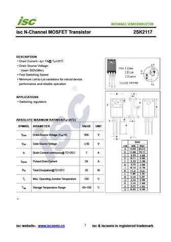
isc N-Channel MOSFET Transistor 2SK2117 DESCRIPTION Drain Current I = 7A@ T =25 D C Drain Source Voltage- V = 500V(Min) DSS Fast Switching Speed Minimum Lot-to-Lot variations for robust device performance and reliable operation APPLICATIONS Switching regulators ABSOLUTE MAXIMUM RATINGS(T =25 ) a SYMBOL ARAMETER VALUE UNIT V Drain-Source Voltage (V =0) 500 V D... See More ⇒
8.1. Size:59K 1
2sk2112.pdf
DATA SHEET MOS FIELD EFFECT TRANSISTOR 2SK2112 N-CHANNEL MOS FET FOR HIGH-SPEED SWITCHING The 2SK2112 is a N-channel MOS FET of a vertical type and PACKAGE DIMENSIONS (in mm) is a switching element that can be directly driven by the output of 4.5 0.1 an IC operating at 5 V. 1.6 0.2 1.5 0.1 This product has a low ON resistance and superb switching characteristics and is idea... See More ⇒
8.2. Size:119K 1
2sk2110.pdf
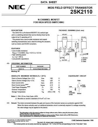
DATA SHEET MOS FIELD EFFECT TRANSISTOR 2SK2110 N-CHANNEL MOSFET FOR HIGH-SPEED SWITCHING DESCRIPTION PACKAGE DRAWING (Unit mm) The 2SK2110 is a N-channel MOSFET of a vertical type 4.5 0.1 and is a switching element that can be directly driven by the output of an IC operating at 5 V. 1.6 0.2 1.5 0.1 This product has a low on-state resistance and superb switching charact... See More ⇒
8.4. Size:33K hitachi
2sk2114 2sk2115.pdf

2SK2114, 2SK2115 Silicon N-Channel MOS FET Application High speed power switching Features Low on-resistance High speed switching Low drive current No secondary breakdown Suitable for Switching regulator Outline TO-220CFM 1 D 2 3 1. Gate G 2. Drain 3. Source S 2SK2114, 2SK2115 Absolute Maximum Ratings (Ta = 25 C) Item Symbol Ratings Unit Drain to so... See More ⇒
8.5. Size:28K hitachi
2sk2118.pdf
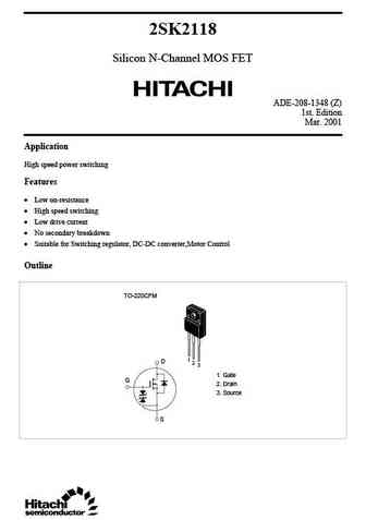
2SK2118 Silicon N-Channel MOS FET ADE-208-1348 (Z) 1st. Edition Mar. 2001 Application High speed power switching Features Low on-resistance High speed switching Low drive current No secondary breakdown Suitable for Switching regulator, DC-DC converter,Motor Control Outline TO-220CFM 1 D 2 3 1. Gate G 2. Drain 3. Source S 2SK2118 Absolute Maximum Rat... See More ⇒
8.6. Size:941K kexin
2sk2112.pdf
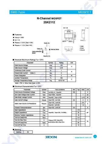
SMD Type MOSFET N-Channel MOSFET 2SK2112 1.70 0.1 Features VDS (V) = 100V ID = 1 A 0.42 0.1 0.46 0.1 RDS(ON) 0.8 (VGS = 10V) Drain (D) RDS(ON) 1.2 (VGS = 4V) 1.Gate 2.Drain Gate (G) Internal diode 3.Source Gate protection diode Source (S) Absolute Maximum Ratings Ta = 25 Parameter Symbol Rating Unit Drain-Source Voltage VDS 100 ... See More ⇒
8.7. Size:937K kexin
2sk2110.pdf
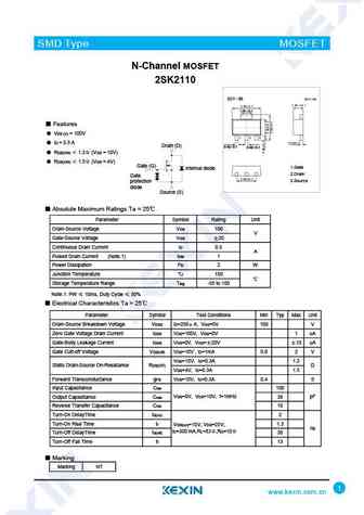
SMD Type MOSFET N-Channel MOSFET 2SK2110 1.70 0.1 Features VDS (V) = 100V ID = 0.5 A Drain (D) 0.42 0.1 0.46 0.1 RDS(ON) 1.2 (VGS = 10V) RDS(ON) 1.5 (VGS = 4V) Gate (G) 1.Gate Internal diode 2.Drain Gate 3.Source protection diode Source (S) Absolute Maximum Ratings Ta = 25 Parameter Symbol Rating Unit Drain-Source Voltage VDS 10... See More ⇒
8.8. Size:662K kexin
2sk2111.pdf
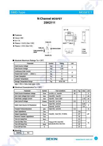
SMD Type MOSFET N-Channel MOSFET 2SK2111 1.70 0.1 Features VDS (V) = 60V ID = 1 A Drain (D) RDS(ON) 0.45 (VGS = 10V) 0.42 0.1 0.46 0.1 RDS(ON) 0.6 (VGS = 4V) Gate (G) Internal diode 1.Gate Gate protection 2.Drain diode 3.Source Source (S) Absolute Maximum Ratings Ta = 25 Parameter Symbol Rating Unit Drain-Source Voltage VDS 60 V ... See More ⇒
8.9. Size:213K inchange semiconductor
2sk2116.pdf
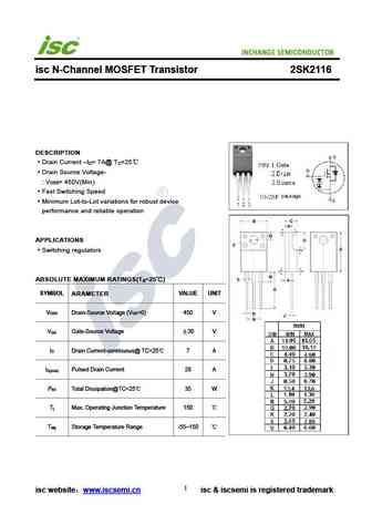
isc N-Channel MOSFET Transistor 2SK2116 DESCRIPTION Drain Current I = 7A@ T =25 D C Drain Source Voltage- V = 450V(Min) DSS Fast Switching Speed Minimum Lot-to-Lot variations for robust device performance and reliable operation APPLICATIONS Switching regulators ABSOLUTE MAXIMUM RATINGS(T =25 ) a SYMBOL ARAMETER VALUE UNIT V Drain-Source Voltage (V =0) 450 V D... See More ⇒
8.10. Size:213K inchange semiconductor
2sk2118.pdf

isc N-Channel MOSFET Transistor 2SK2118 DESCRIPTION Drain Current I = 5A@ T =25 D C Drain Source Voltage- V = 600V(Min) DSS Fast Switching Speed Minimum Lot-to-Lot variations for robust device performance and reliable operation APPLICATIONS Switching regulators ,DC-DC converter,Motor Control ABSOLUTE MAXIMUM RATINGS(T =25 ) a SYMBOL ARAMETER VALUE UNIT V Drain... See More ⇒
8.11. Size:212K inchange semiconductor
2sk2114.pdf
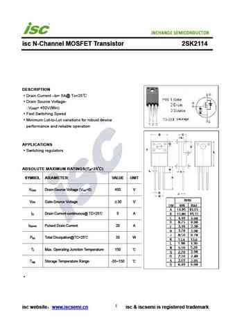
isc N-Channel MOSFET Transistor 2SK2114 DESCRIPTION Drain Current I = 5A@ T =25 D C Drain Source Voltage- V = 450V(Min) DSS Fast Switching Speed Minimum Lot-to-Lot variations for robust device performance and reliable operation APPLICATIONS Switching regulators ABSOLUTE MAXIMUM RATINGS(T =25 ) a SYMBOL ARAMETER VALUE UNIT V Drain-Source Voltage (V =0) 450 V D... See More ⇒
8.12. Size:212K inchange semiconductor
2sk2115.pdf
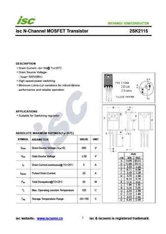
isc N-Channel MOSFET Transistor 2SK2115 DESCRIPTION Drain Current I = 5A@ T =25 D C Drain Source Voltage- V = 500V(Min) DSS High speed power switching Minimum Lot-to-Lot variations for robust device performance and reliable operation APPLICATIONS Suitable for Switching regulator ABSOLUTE MAXIMUM RATINGS(T =25 ) a SYMBOL ARAMETER VALUE UNIT V Drain-Source Volta... See More ⇒
Detailed specifications: 2SK2024-01, 2SK2025, 2SK2026-01, 2SK2028-01MR, 2SK2050, 2SK2052, 2SK2080-01, 2SK2116, AON7506, 2SK2118, 2SK2144, 2SK2147-01, 2SK2148-01, 2SK2180-01, 2SK2223-01, 2SK2224-01, 2SK2251-01
Keywords - 2SK2117 MOSFET specs
2SK2117 cross reference
2SK2117 equivalent finder
2SK2117 pdf lookup
2SK2117 substitution
2SK2117 replacement
Need a MOSFET replacement?
Our guide shows you how to find a perfect substitute by comparing key parameters and specs