MTP23P06VG Datasheet. Specs and Replacement
Type Designator: MTP23P06VG 📄📄
Type of Transistor: MOSFET
Type of Control Channel: P-Channel
Absolute Maximum Ratings
Pd ⓘ - Maximum Power Dissipation: 90 W
|Vds|ⓘ - Maximum Drain-Source Voltage: 60 V
|Vgs|ⓘ - Maximum Gate-Source Voltage: 15 V
|Id| ⓘ - Maximum Drain Current: 23 A
Tj ⓘ - Maximum Junction Temperature: 175 °C
Electrical Characteristics
tr ⓘ - Rise Time: 98.3 nS
Cossⓘ - Output Capacitance: 380 pF
RDSonⓘ - Maximum Drain-Source On-State Resistance: 0.12 Ohm
Package: TO-220AB
📄📄 Copy
MTP23P06VG substitution
- MOSFET ⓘ Cross-Reference Search
MTP23P06VG datasheet
mtp23p06v mtp23p06v mtp23p06vg.pdf
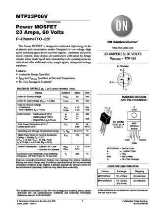
MTP23P06V Preferred Device Power MOSFET 23 Amps, 60 Volts P-Channel TO-220 This Power MOSFET is designed to withstand high energy in the http //onsemi.com avalanche and commutation modes. Designed for low voltage, high speed switching applications in power supplies, converters and power 23 AMPERES, 60 VOLTS motor controls, these devices are particularly well suited for bridge RDS(on)... See More ⇒
mtp23p06v.pdf

MOTOROLA Order this document SEMICONDUCTOR TECHNICAL DATA by MTP23P06V/D Designer's Data Sheet MTP23P06V TMOS V Motorola Preferred Device Power Field Effect Transistor P Channel Enhancement Mode Silicon Gate TMOS POWER FET TMOS V is a new technology designed to achieve an on resis- 23 AMPERES tance area product about one half that of standard MOSFETs. This 60 VOLTS ... See More ⇒
mtp23p06vrev1e.pdf
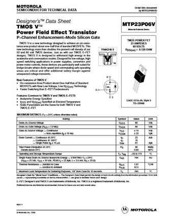
MOTOROLA Order this document SEMICONDUCTOR TECHNICAL DATA by MTP23P06V/D Designer's Data Sheet MTP23P06V TMOS V Motorola Preferred Device Power Field Effect Transistor P Channel Enhancement Mode Silicon Gate TMOS POWER FET TMOS V is a new technology designed to achieve an on resis- 23 AMPERES tance area product about one half that of standard MOSFETs. This 60 VOLTS ... See More ⇒
mtp2311m3.pdf
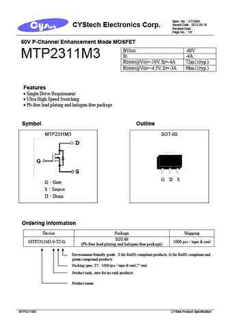
Spec. No. C733M3 Issued Date 2013.09.18 CYStech Electronics Corp. Revised Date Page No. 1/9 60V P-Channel Enhancement Mode MOSFET BVDSS -60V ID -4A MTP2311M3 RDSON@VGS=-10V, ID=-4A 72m (typ.) RDSON@VGS=-4.5V, ID=-3A 98m (typ.) Features Single Drive Requirement Ultra High Speed Switching Pb-free lead plating and halogen-free package Symbol Outlin... See More ⇒
Detailed specifications: MTP1N60E, MTP1N80E, MTP1N95, MTP20N10E, MTP20N15EG, MTP20N20E, MTP20P06, MTP23P06V, K4145, MTP25N05E, MTP2955, MTP2955V, MTP2N18, MTP2N20, MTP2N35, MTP2N40, MTP2N40E
Keywords - MTP23P06VG MOSFET specs
MTP23P06VG cross reference
MTP23P06VG equivalent finder
MTP23P06VG pdf lookup
MTP23P06VG substitution
MTP23P06VG replacement
Step-by-step guide to finding a MOSFET replacement. Cross-reference parts and ensure compatibility for your repair or project.
MOSFET Parameters. How They Affect Each Other
History: NCE65T1K2K | SVF13N50PN
🌐 : EN ES РУ

LIST
Last Update
MOSFET: CS95118 | CS85105A | CS75N45 | CS72N12 | CS55N50 | CS48N75A | CS40N27 | MSQ60P04D | MSQ40P07D | MSQ30P40D
Popular searches
oc70 transistor | p0603bd mosfet | p157r5nt | ptp03n04n | sm4377 mosfet datasheet | tip31c reemplazo | 2sa906 | c2389 transistor