IPI030N10N3 Specs and Replacement
Type Designator: IPI030N10N3
Type of Transistor: MOSFET
Type of Control Channel: N-Channel
Absolute Maximum Ratings
Pd ⓘ - Maximum Power Dissipation: 300 W
|Vds|ⓘ - Maximum Drain-Source Voltage: 100 V
|Vgs|ⓘ - Maximum Gate-Source Voltage: 20 V
|Id| ⓘ - Maximum Drain Current: 100 A
Tj ⓘ - Maximum Junction Temperature: 175 °C
Electrical Characteristics
tr ⓘ - Rise Time: 58 nS
Cossⓘ - Output Capacitance: 1940 pF
RDSonⓘ - Maximum Drain-Source On-State Resistance: 0.003 Ohm
Package: TO-262
IPI030N10N3 substitution
- MOSFET ⓘ Cross-Reference Search
IPI030N10N3 datasheet
ipi030n10n3.pdf
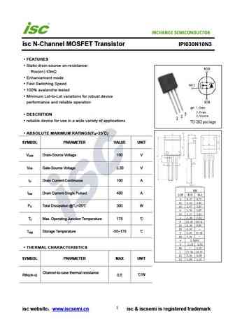
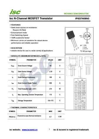
INCHANGE Semiconductor isc N-Channel MOSFET Transistor IPI030N10N3 FEATURES Static drain-source on-resistance RDS(on) 3m Enhancement mode Fast Switching Speed 100% avalanche tested Minimum Lot-to-Lot variations for robust device performance and reliable operation DESCRITION reliable device for use in a wide variety of applications ABSOLUTE MAXIMUM RATINGS(T ... See More ⇒
ipi030n10n3g ipp030n10n3g ipp030n10n3g ipi030n10n3g.pdf
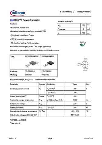
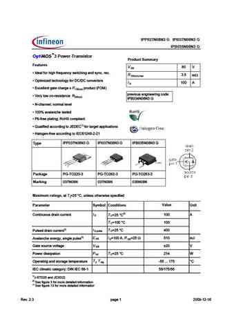
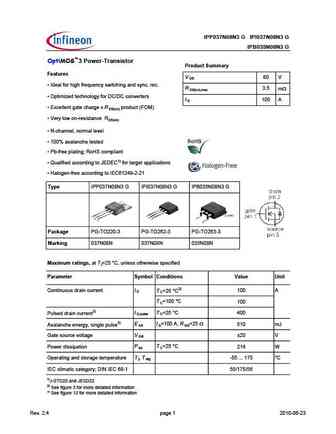
IPP030N10N3 G IPI030N10N3 G OptiMOS 3 Power-Transistor Product Summary Features VDS 100 V N-channel, normal level RDS(on),max 3 mW Excellent gate charge x R product (FOM) DS(on) ID 100 A Very low on-resistance R DS(on) 175 C operating temperature Pb-free lead plating; RoHS compliant Qualified according to JEDEC1) for target application Ideal for h... See More ⇒
ipi034ne7n3g ipp034ne7n3g.pdf
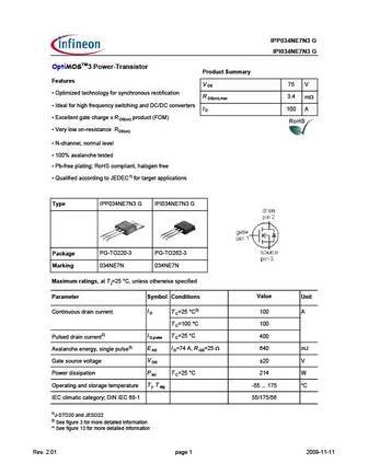
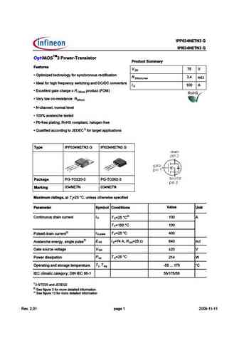
IPP034NE7N3 G IPI034NE7N3 G OptiMOSTM3 Power-Transistor Product Summary Features V 75 V DS Optimized technology for synchronous rectification R 3.4 m DS(on),max Ideal for high frequency switching and DC/DC converters I 100 A D Excellent gate charge x R product (FOM) DS(on) Very low on-resistance RDS(on) N-channel, normal level 100% avalanche tested ... See More ⇒
ipb034n06l3g ipi037n06l3g ipp037n06l3g.pdf
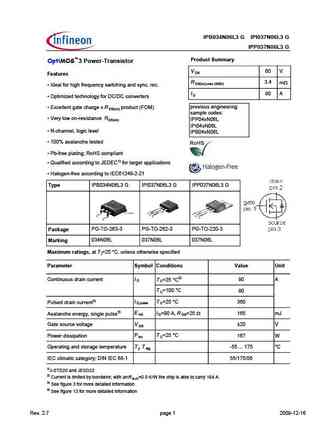
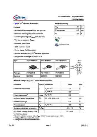
Type IPB034N06L3 G IPI037N06L3 G IPP037N06L3 G Product Summary OptiMOS 3 Power-Transistor V 60 V DS Features R 3.4 m DS(on),max (SMD) Ideal for high frequency switching and sync. rec. I 90 A D Optimized technology for DC/DC converters previous engineering Excellent gate charge x R product (FOM) DS(on) sample codes Very low on-resistance RDS(on) IPP04xN06... See More ⇒
Detailed specifications: IPA037N08N3, IPA045N10N3, IPA057N08N3, IPA086N10N3, IPA60R180C7, IPA60R360P7, IPAN60R650CE, IPB048N15N5, IRF540N, IPI037N08N3, IPI041N12N3, IPI051N15N5, IPI072N10N3, IPI075N15N3, IPI076N12N3, IPI076N15N5, IPI086N10N3
Keywords - IPI030N10N3 MOSFET specs
IPI030N10N3 cross reference
IPI030N10N3 equivalent finder
IPI030N10N3 pdf lookup
IPI030N10N3 substitution
IPI030N10N3 replacement
Need a MOSFET replacement? Our guide shows you how to find a perfect substitute by comparing key parameters and specs
History: TPH2900ENH | VB1240B
🌐 : EN ES РУ

LIST
Last Update
MOSFET: AUB062N08BG | AUB060N08AG | AUB056N10 | AUB056N08BGL | AUB050N085 | AUB050N055 | AUB045N12 | AUB045N10BT | AUB039N10 | AUB034N10
Popular searches
2sb817 | mn2488 datasheet | c2026 transistor | 2n3903 transistor | 2n4360 | 2n2613 | c2166 transistor | 2sd330