APT6013LFLL Datasheet. Specs and Replacement
Type Designator: APT6013LFLL 📄📄
Type of Transistor: MOSFET
Type of Control Channel: N-Channel
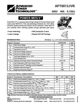
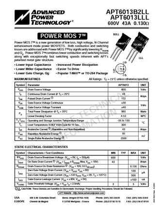
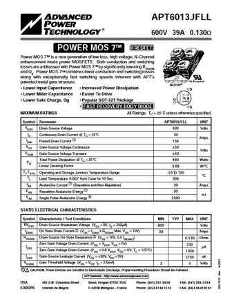
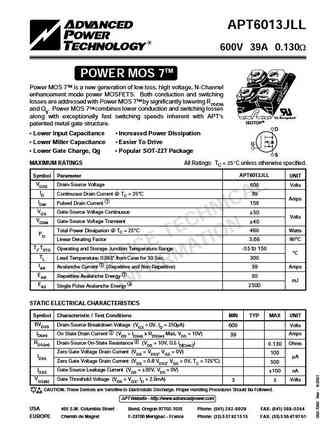
Absolute Maximum Ratings
Pd ⓘ - Maximum Power Dissipation: 565 W
|Vds|ⓘ - Maximum Drain-Source Voltage: 600 V
|Vgs|ⓘ - Maximum Gate-Source Voltage: 30 V
|Id| ⓘ - Maximum Drain Current: 43 A
Tj ⓘ - Maximum Junction Temperature: 150 °C
Electrical Characteristics
tr ⓘ - Rise Time: 14 nS
Cossⓘ - Output Capacitance: 1060 pF
RDSonⓘ - Maximum Drain-Source On-State Resistance: 0.13 Ohm
Package: TO264
📄📄 Copy
APT6013LFLL substitution
- MOSFET ⓘ Cross-Reference Search
APT6013LFLL datasheet
apt6013lfll.pdf
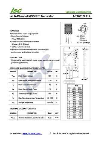
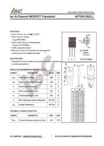
isc N-Channel MOSFET Transistor APT6013LFLL FEATURES Drain Current I = 43A@ T =25 D C Drain Source Voltage- V =600V(Min) DSS Static Drain-Source On-Resistance R =0.13 (Max) DS(on) 100% avalanche tested Minimum Lot-to-Lot variations for robust device performance and reliable operation DESCRIPTION Designed for use in switch mode power supplies and general pur... See More ⇒
apt6013b2fllg apt6013lfllg.pdf
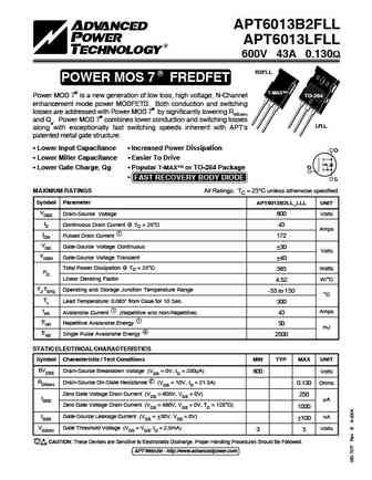
APT6013B2FLL APT6013LFLL 600V 43A 0.130 B2FLL R POWER MOS 7 FREDFET T-MAX TO-264 Power MOS 7 is a new generation of low loss, high voltage, N-Channel enhancement mode power MOSFETS. Both conduction and switching losses are addressed with Power MOS 7 by significantly lowering RDS(ON) and Qg. Power MOS 7 combines lower conduction and switching losses L... See More ⇒
apt6013b2llg apt6013lllg.pdf
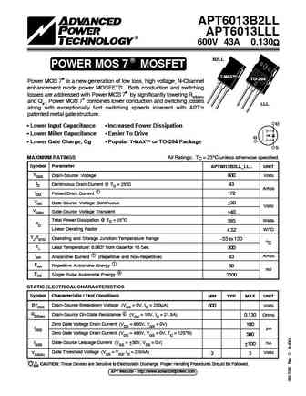
APT6013B2LL APT6013LLL 600V 43A 0.130 B2LL R POWER MOS 7 MOSFET T-MAX TO-264 Power MOS 7 is a new generation of low loss, high voltage, N-Channel enhancement mode power MOSFETS. Both conduction and switching losses are addressed with Power MOS 7 by significantly lowering RDS(ON) and Qg. Power MOS 7 combines lower conduction and switching losses LLL ... See More ⇒
apt6013b2fll.pdf
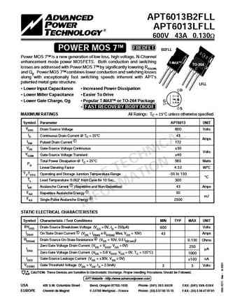
APT6013B2FLL APT6013LFLL 600V 43A 0.130W TM FREDFET POWER MOS 7 B2FLL Power MOS 7TM is a new generation of low loss, high voltage, N-Channel enhancement mode power MOSFETS. Both conduction and switching T-MAX TO-264 losses are addressed with Power MOS 7TM by significantly lowering RDS(ON) and Qg. Power MOS 7TM combines lower conduction and switching losses along with exceptiona... See More ⇒

Detailed specifications: APT47N65BC3, APT5010LFLL, APT5010LLL, APT5015BVFR, APT50M75LFLL, APT50M80LVFR, APT6010B2FLL, APT6010LFLL, 2N60, APT6015B2VFR, APT6017LFLL, APT60N60BCS, R6004KNJ, R6004KNX, R6007KNJ, R6007KNX, R6007MNJ
Keywords - APT6013LFLL MOSFET specs
APT6013LFLL cross reference
APT6013LFLL equivalent finder
APT6013LFLL pdf lookup
APT6013LFLL substitution
APT6013LFLL replacement
Learn how to find the right MOSFET substitute. A guide to cross-reference, check specs and replace MOSFETs in your circuits.
MOSFET Parameters. How They Affect Each Other
History: HM7N60F | APTM100A13SCG | SSW65R075SFD2 | JMSH1018PGD | QM03N65D | BF244B | IPD200N15N3G
🌐 : EN ES РУ

LIST
Last Update
MOSFET: CS95118 | CS85105A | CS75N45 | CS72N12 | CS55N50 | CS48N75A | CS40N27 | MSQ60P04D | MSQ40P07D | MSQ30P40D
Popular searches
tip141 | 2n404 | 2n4250 | d882 transistor equivalent | 17n80c3 | bc107 transistor | rjp63g4 datasheet | 2sc1115