SI2333 Specs and Replacement
Type Designator: SI2333
Type of Transistor: MOSFET
Type of Control Channel: P-Channel
Absolute Maximum Ratings
Pd ⓘ
- Maximum Power Dissipation: 1.1 W
|Vds|ⓘ - Maximum Drain-Source Voltage: 12 V
|Vgs|ⓘ - Maximum Gate-Source Voltage: 8 V
|Id| ⓘ - Maximum Drain Current: 6 A
Tj ⓘ - Maximum Junction Temperature: 150 °C
Electrical Characteristics
tr ⓘ - Rise Time: 24 nS
Cossⓘ -
Output Capacitance: 255 pF
RDSonⓘ - Maximum Drain-Source On-State Resistance: 0.028 Ohm
Package: SOT23
- MOSFET ⓘ Cross-Reference Search
SI2333 datasheet
..1. Size:984K mcc
si2333.pdf 
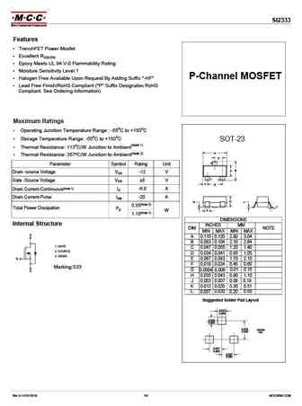
SI2333 Features TrenchFET Power Mosfet Excellent RDS(ON) Epoxy Meets UL 94 V-0 Flammability Rating Moisture Sensitivity Level 1 P-Channel MOSFET Halogen Free Available Upon Request By Adding Suffix "-HF" Lead Free Finish/RoHS Compliant ("P" Suffix Designates RoHS Compliant. See Ordering Information) Maximum Ratings Operating Junction Temperature Range -5... See More ⇒
..2. Size:1409K born
si2333.pdf
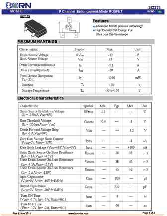
SI2333 MOSFET ROHS P-Channel Enhancement-Mode MOSFET SOT-23 - Features Advanced trench process technology High Density Cell Design For Ultra Low On-Resistance MAXIMUM RANTINGS Characteristic Symbol Max Unit Drain-Source Voltage BV -12 V DSS Gate- Source Voltage V +8 V GS Drain Current (continuous) I -5.1 A D Drain Current (pulsed) I -20 A DM Total Device Dissipa... See More ⇒
0.1. Size:226K vishay
si2333dds.pdf
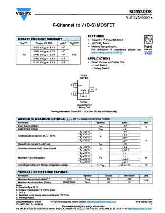
Si2333DDS Vishay Siliconix P-Channel 12 V (D-S) MOSFET FEATURES MOSFET PRODUCT SUMMARY TrenchFET Power MOSFET VDS (V) RDS(on) ( ) Max. ID (A)a Qg (Typ.) 100 % Rg Tested Material categorization 0.028 at VGS = - 4.5 V - 6e For definitions of compliance please see 0.032 at VGS = - 3.7 V - 6e www.vishay.com/doc?99912 - 12 0.040 at VGS = - 2.5 V - 6e 9 nC 0.063 at... See More ⇒
0.2. Size:186K vishay
si2333ds.pdf
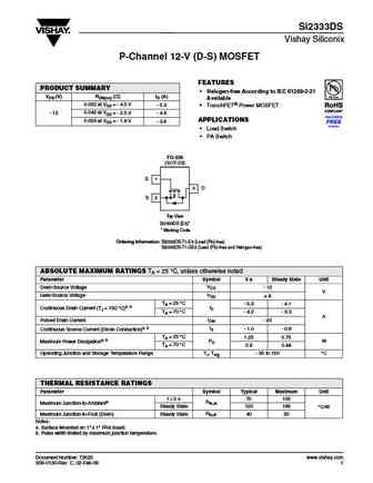
Si2333DS Vishay Siliconix P-Channel 12-V (D-S) MOSFET FEATURES PRODUCT SUMMARY Halogen-free According to IEC 61249-2-21 VDS (V) RDS(on) ( )ID (A) Available 0.032 at VGS = - 4.5 V - 5.3 TrenchFET Power MOSFET 0.042 at VGS = - 2.5 V - 12 - 4.6 APPLICATIONS 0.059 at VGS = - 1.8 V - 3.9 Load Switch PA Switch TO-236 (SOT-23) G 1 3 D S 2 Top View S... See More ⇒
0.3. Size:224K vishay
si2333cds.pdf
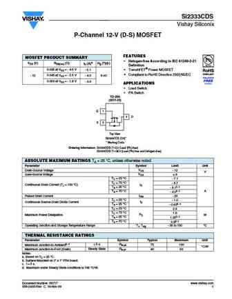
Si2333CDS Vishay Siliconix P-Channel 12-V (D-S) MOSFET FEATURES MOSFET PRODUCT SUMMARY Halogen-free According to IEC 61249-2-21 VDS (V) RDS(on) ( ) ID (A)a Qg (Typ.) Definition 0.035 at VGS = - 4.5 V - 5.1 TrenchFET Power MOSFET Compliant to RoHS Directive 2002/95/EC 0.045 at VGS = - 2.5 V - 4.5 9 nC - 12 0.059 at VGS = - 1.8 V - 3.9 APPLICATIONS Load Switc... See More ⇒
0.4. Size:216K vishay
si2333cd.pdf

Si2333CDS Vishay Siliconix P-Channel 12-V (D-S) MOSFET FEATURES MOSFET PRODUCT SUMMARY Halogen-free According to IEC 61249-2-21 VDS (V) RDS(on) ( ) ID (A)a Qg (Typ.) Definition 0.035 at VGS = - 4.5 V - 5.1 TrenchFET Power MOSFET Compliant to RoHS Directive 2002/95/EC 0.045 at VGS = - 2.5 V - 4.5 9 nC - 12 0.059 at VGS = - 1.8 V - 3.9 APPLICATIONS Load Switc... See More ⇒
0.5. Size:1947K kexin
si2333cds ki2333cds.pdf
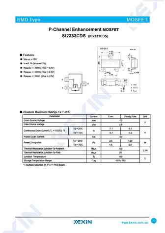
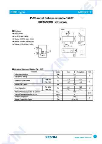
SMD Type MOSFET P-Channel Enhancement MOSFET SI2333CDS (KI2333CDS) SOT-23-3 Unit mm +0.2 2.9-0.1 +0.1 0.4 -0.1 Features 3 VDS (V) =-12V ID =-5.1A (VGS =-4.5V) RDS(ON) 35m (VGS =-4.5V) 1 2 +0.02 +0.1 RDS(ON) 45m (VGS =-2.5V) 0.15 -0.02 0.95 -0.1 +0.1 1.9-0.2 RDS(ON) 59m (VGS =-1.8V) G 1 3 D 1. Gate 2. Source S 2 3. D... See More ⇒
0.6. Size:1223K kexin
si2333ds.pdf

SMD Type MOSFET P-Channel MOSFET SI2333DS (KI2333DS) SOT-23 Unit mm +0.1 2.9-0.1 +0.1 0.4 -0.1 3 Features VDS (V) =-12V ID =-5.3 A (VGS =-4.5V) 1 2 RDS(ON) 32m (VGS =-4.5V) +0.1 +0.05 0.95 -0.1 0.1 -0.01 1.9+0.1 -0.1 RDS(ON) 42m (VGS =-2.5V) RDS(ON) 59m (VGS =-1.8V) 1. Gate 2. Source 3. Drain G 1 3 D S 2 Absolute Max... See More ⇒
0.8. Size:1240K kexin
si2333ds-3.pdf
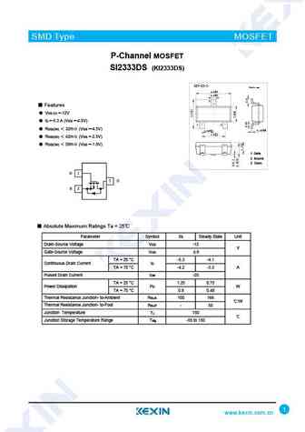
SMD Type MOSFET P-Channel MOSFET SI2333DS (KI2333DS) SOT-23-3 Unit mm +0.2 2.9-0.1 +0.1 0.4 -0.1 3 Features VDS (V) =-12V ID =-5.3 A (VGS =-4.5V) 1 2 RDS(ON) 32m (VGS =-4.5V) +0.02 +0.1 0.15 -0.02 0.95 -0.1 +0.1 1.9-0.2 RDS(ON) 42m (VGS =-2.5V) RDS(ON) 59m (VGS =-1.8V) 1. Gate 2. Source 3. Drain G 1 3 D S 2 Absolute... See More ⇒
0.9. Size:1947K kexin
si2333cds-3.pdf

SMD Type MOSFET P-Channel Enhancement MOSFET SI2333CDS (KI2333CDS) SOT-23-3 Unit mm +0.2 2.9-0.1 +0.1 0.4 -0.1 Features 3 VDS (V) =-12V ID =-5.1A (VGS =-4.5V) RDS(ON) 35m (VGS =-4.5V) 1 2 +0.02 +0.1 RDS(ON) 45m (VGS =-2.5V) 0.15 -0.02 0.95 -0.1 +0.1 1.9-0.2 RDS(ON) 59m (VGS =-1.8V) G 1 3 D 1. Gate 2. Source S 2 3. D... See More ⇒
0.10. Size:1472K cn vbsemi
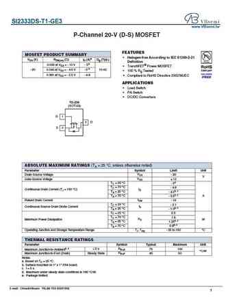
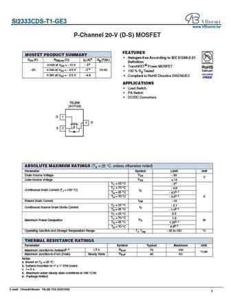
si2333dds-t1.pdf
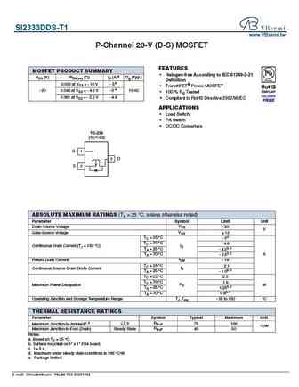
SI2333DDS-T1 www.VBsemi.tw P-Channel 20-V (D-S) MOSFET FEATURES MOSFET PRODUCT SUMMARY Halogen-free According to IEC 61249-2-21 VDS (V) RDS(on) ( )ID (A)a Qg (Typ.) Definition 0.035 at VGS = - 10 V - 5e TrenchFET Power MOSFET e - 20 0.043 at VGS = - 4.5 V - 5 10 nC 100 % Rg Tested 0.061 at VGS = - 2.5 V - 4.8 Compliant to RoHS Directive 2002/95/EC APPLICATION... See More ⇒
0.11. Size:866K cn vbsemi
si2333ds-t1-ge3.pdf
SI2333DS-T1-GE3 www.VBsemi.tw P-Channel 20-V (D-S) MOSFET FEATURES MOSFET PRODUCT SUMMARY Halogen-free According to IEC 61249-2-21 VDS (V) RDS(on) ( )ID (A)a Qg (Typ.) Definition 0.035 at VGS = - 10 V - 5e TrenchFET Power MOSFET e - 20 0.043 at VGS = - 4.5 V - 5 10 nC 100 % Rg Tested 0.061 at VGS = - 2.5 V - 4.8 Compliant to RoHS Directive 2002/95/EC APPLICAT... See More ⇒
0.12. Size:866K cn vbsemi
si2333cds-t1-ge3.pdf
SI2333CDS-T1-GE3 www.VBsemi.tw P-Channel 20-V (D-S) MOSFET FEATURES MOSFET PRODUCT SUMMARY Halogen-free According to IEC 61249-2-21 VDS (V) RDS(on) ( )ID (A)a Qg (Typ.) Definition 0.035 at VGS = - 10 V - 5e TrenchFET Power MOSFET e - 20 0.043 at VGS = - 4.5 V - 5 10 nC 100 % Rg Tested 0.061 at VGS = - 2.5 V - 4.8 Compliant to RoHS Directive 2002/95/EC APPLICA... See More ⇒
Detailed specifications: BM3407A, BM3415E, BM3416E, BML6401, BML6402, SI2301-P, SI2301S, SI2302S, IRFP260N, ASDM20N12ZB, ASDM20P09ZB, ASDM2301ZA, ASDM3010, ASDM3010S, ASDM3020, ASDM3050, ASDM3080KQ
Keywords - SI2333 MOSFET specs
SI2333 cross reference
SI2333 equivalent finder
SI2333 pdf lookup
SI2333 substitution
SI2333 replacement
Step-by-step guide to finding a MOSFET replacement. Cross-reference parts and ensure compatibility for your repair or project.