ASDM3010S Specs and Replacement
Type Designator: ASDM3010S
Type of Transistor: MOSFET
Type of Control Channel: N-Channel
Absolute Maximum Ratings
Pd ⓘ
- Maximum Power Dissipation: 2.5 W
|Vds|ⓘ - Maximum Drain-Source Voltage: 30 V
|Vgs|ⓘ - Maximum Gate-Source Voltage: 20 V
|Id| ⓘ - Maximum Drain Current: 9 A
Tj ⓘ - Maximum Junction Temperature: 150 °C
Electrical Characteristics
tr ⓘ - Rise Time: 7 nS
Cossⓘ -
Output Capacitance: 95 pF
RDSonⓘ - Maximum Drain-Source On-State Resistance: 0.02 Ohm
Package: SOP8
- MOSFET ⓘ Cross-Reference Search
ASDM3010S datasheet
..1. Size:516K ascend
asdm3010s.pdf 

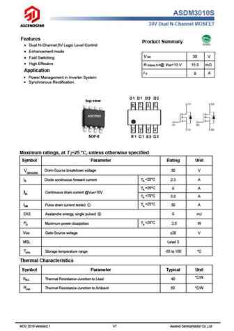
ASDM3010S 30V Dual N-Channel MOSFET Features Product Summary Dual N-Channel,5V Logic Level Control Enhancement mode V DS 30 V Fast Switching High Effective R DS(on),TYP@ VGS=10 V 15.5 m Application I D 9 A Power Management in Inverter System Synchronous Rectification top view ASCEND SOP-8 Maximum ratings, at T j=25 C, unless otherwise specified S... See More ⇒
6.1. Size:1008K ascend
asdm3010.pdf 

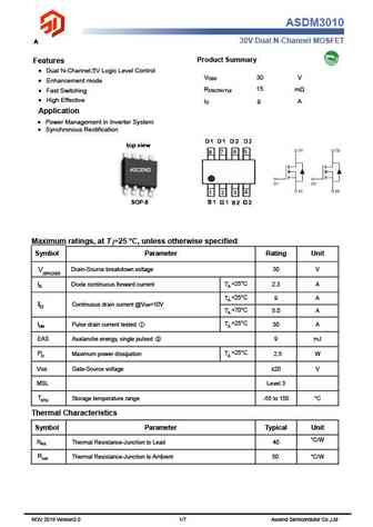
ASDM3010 30V Dual N-Channel MOSFET Product Summary Features Dual N-Channel,5V Logic Level Control V 30 V DSS Enhancement mode 15 R m DS(ON)-Typ Fast Switching High Effective I A D 9 Application Power Management in Inverter System Synchronous Rectification top view ASCEND SOP-8 Maximum ratings, at T j=25 C, unless otherwise specified Symbol ... See More ⇒
8.1. Size:435K 1
asdm30p30ctd-r.pdf 

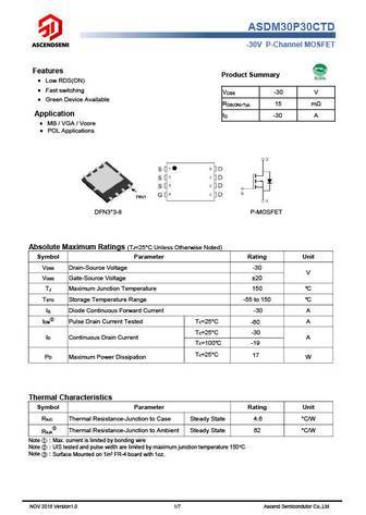
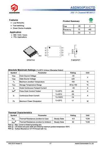
ASDM30P30CTD -30V P-Channel MOSFET Features Product Summary Low RDS(ON) Fast switching V -30 V DSS Green Device Available R 15 m DS(ON)-Typ. Application I -30 A D MB / VGA / Vcore POL Applications DFN3*3-8 P-MOSFET Absolute Maximum Ratings (T =25 C Unless Otherwise Noted) J Symbol Parameter Rating Unit VDSS Drain-Source Voltage -30 V VGSS Gate-... See More ⇒
8.2. Size:577K 1
asdm30p30ctd.pdf 

ASDM30P30CTD -30V P-Channel MOSFET Features Product Summary Low RDS(ON) Fast switching V -30 V DSS Green Device Available R 15 m DS(ON)-Typ. Application I -30 A D MB / VGA / Vcore POL Applications DFN3*3-8 P-MOSFET Absolute Maximum Ratings (T =25 C Unless Otherwise Noted) J Symbol Parameter Rating Unit VDSS Drain-Source Voltage -30 V VGSS Gate-... See More ⇒
8.3. Size:514K 1
asdm30p11td-r.pdf 

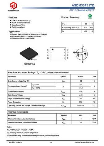
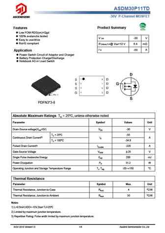
ASDM30P11TD -30V P-Channel MOSFET Product Summary Features Low FOM RDS(on) Qgd 100% avalanche tested V DS -30 V Easy to use/drive RoHS compliant R DS(on),TYP@ VGS=10 V 6.4 m I D -55 A Application Power Switch Circuit of Adaptor and Charger Battery Protection Charge/Discharge Notebook AC-in Load Switch PDFN3*3-8 Absolute Maximum Ratings TA = 25 u... See More ⇒
8.4. Size:315K 1
asdm30n65e-r.pdf 

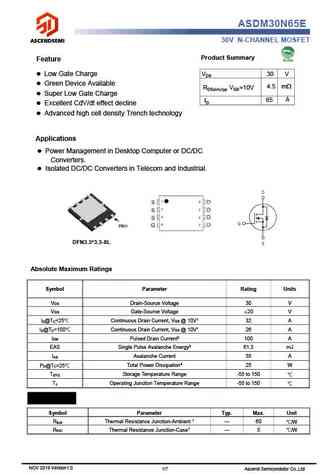
ASDM30N65E 30V N-CHANNEL MOSFET Product Summary Feature l Low Gate Charge VDS 30 V l Green Device Available 4.5 m RDS(on),typ VGS=10V l Super Low Gate Charge A 65 ID l Excellent CdV/dt effect decline l Advanced high cell density Trench technology Applications l Power Management in Desktop Computer or DC/DC Converters. l Isolated DC/DC Converters in Telecom and Industrial. ... See More ⇒
8.5. Size:348K 1
asdm30n55e-r.pdf 

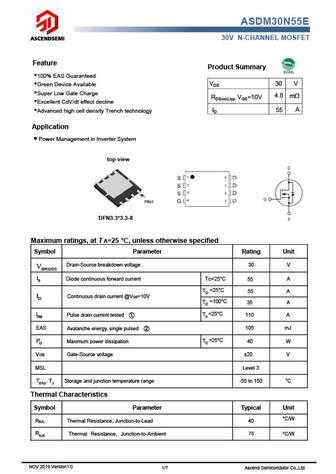
ASDM30N55E 30V N-CHANNEL MOSFET Feature Product Summary 100% EAS Guaranteed VDS 30 V Green Device Available Super Low Gate Charge RDS(on),typ VGS=10V 4.8 m Excellent CdV/dt effect decline A 55 ID Advanced high cell density Trench technology Application Power Management in Inverter System top view DFN3.3*3.3-8 Maximum ratings, at T A=25 C, unless othe... See More ⇒
8.6. Size:285K ascend
asdm3080kq.pdf 

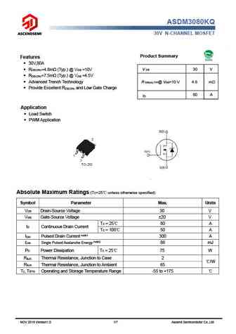
ASDM3080KQ 30V N-CHANNEL MOSFET Product Summary Features 30V,80A R =4.8m (Typ.) @ V =10V V DS 30 V DS(ON) GS R =7.5m (Typ.) @ V =4.5V DS(ON) GS Advanced Trench Technology R DS(on),TYP@ VGS=10 V 4.8 m Provide Excellent R and Low Gate Charge DS(ON) 80 A ID Application Load Switch PWM Application Absolute Maximum Ratings (T =25 unless othe... See More ⇒
8.7. Size:435K ascend
asdm30p30ctd.pdf 

ASDM30P30CTD -30V P-Channel MOSFET Features Product Summary Low RDS(ON) Fast switching V -30 V DSS Green Device Available R 15 m DS(ON)-Typ. Application I -30 A D MB / VGA / Vcore POL Applications DFN3*3-8 P-MOSFET Absolute Maximum Ratings (T =25 C Unless Otherwise Noted) J Symbol Parameter Rating Unit VDSS Drain-Source Voltage -30 V VGSS Gate-... See More ⇒
8.8. Size:521K ascend
asdm3020.pdf 

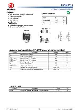
ASDM3020 30V Dual N-Channel MOSFET Features Product Summary Dual N-Channel,5V Logic Level Control Enhancement mode V 30 V DSS Fast Switching 11.5 R m DS(ON)-Max High Effective I A D 11.8 Application Power Management in Inverter System Synchronous Rectification top view ASCEND SOP-8 NOV 2018 Version1.0 1/7 Ascend Semicondutor Co.,Ltd ASDM3020... See More ⇒
8.9. Size:315K ascend
asdm30n65e.pdf 

ASDM30N65E 30V N-CHANNEL MOSFET Product Summary Feature l Low Gate Charge VDS 30 V l Green Device Available 4.5 m RDS(on),typ VGS=10V l Super Low Gate Charge A 65 ID l Excellent CdV/dt effect decline l Advanced high cell density Trench technology Applications l Power Management in Desktop Computer or DC/DC Converters. l Isolated DC/DC Converters in Telecom and Industrial. ... See More ⇒
8.10. Size:303K ascend
asdm30n90kq.pdf 

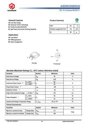
ASDM30N90KQ 30V N-Channel MOSFET General Features Product Summary Low Gate Charge Advanced Trench Technology VDS 30 V Provide Excellent RDS(ON) RDS(on),Typ.@ VGS=10 V 3.6 m High Power and Current Handling Capability 90 ID A Application Load Swtich PWM applications Power management 1 TO-252 N-channel Absolute Maximum Ratings (TA =25 C unless o... See More ⇒
8.11. Size:514K ascend
asdm30p11td.pdf 

ASDM30P11TD -30V P-Channel MOSFET Product Summary Features Low FOM RDS(on) Qgd 100% avalanche tested V DS -30 V Easy to use/drive RoHS compliant R DS(on),TYP@ VGS=10 V 6.4 m I D -55 A Application Power Switch Circuit of Adaptor and Charger Battery Protection Charge/Discharge Notebook AC-in Load Switch PDFN3*3-8 Absolute Maximum Ratings TA = 25 u... See More ⇒
8.12. Size:348K ascend
asdm30n55e.pdf 

ASDM30N55E 30V N-CHANNEL MOSFET Feature Product Summary 100% EAS Guaranteed VDS 30 V Green Device Available Super Low Gate Charge RDS(on),typ VGS=10V 4.8 m Excellent CdV/dt effect decline A 55 ID Advanced high cell density Trench technology Application Power Management in Inverter System top view DFN3.3*3.3-8 Maximum ratings, at T A=25 C, unless othe... See More ⇒
8.14. Size:740K ascend
asdm3050.pdf 

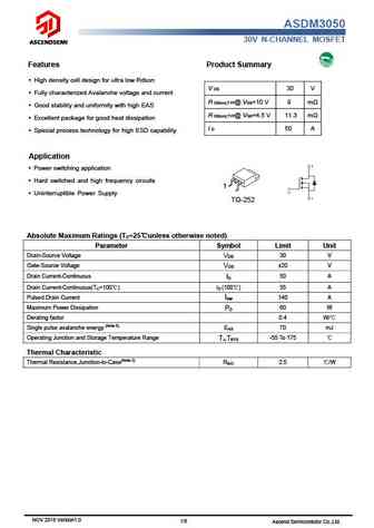
ASDM3050 30V N-CHANNEL MOSFET Features Product Summary High density cell design for ultra low Rdson V DS 30 V Fully characterized Avalanche voltage and current R DS(on),TYP@ VGS=10 V 9 m Good stability and uniformity with high EAS R DS(on),TYP@ VGS=4.5 V 11.3 m Excellent package for good heat dissipation I D 50 A Special process technology for high ESD ... See More ⇒
Detailed specifications: SI2301-P, SI2301S, SI2302S, SI2333, ASDM20N12ZB, ASDM20P09ZB, ASDM2301ZA, ASDM3010, AON6414A, ASDM3020, ASDM3050, ASDM3080KQ, ASDM30N55E, ASDM30N65E, ASDM30N90KQ, ASDM30P09ZB, ASDM30P11TD
Keywords - ASDM3010S MOSFET specs
ASDM3010S cross reference
ASDM3010S equivalent finder
ASDM3010S pdf lookup
ASDM3010S substitution
ASDM3010S replacement
Learn how to find the right MOSFET substitute. A guide to cross-reference, check specs and replace MOSFETs in your circuits.
