SSF10N80A Datasheet. Specs and Replacement
Type Designator: SSF10N80A 📄📄
Type of Transistor: MOSFET
Type of Control Channel: N-Channel
Absolute Maximum Ratings
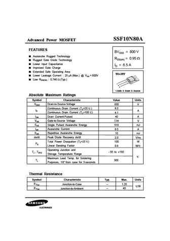
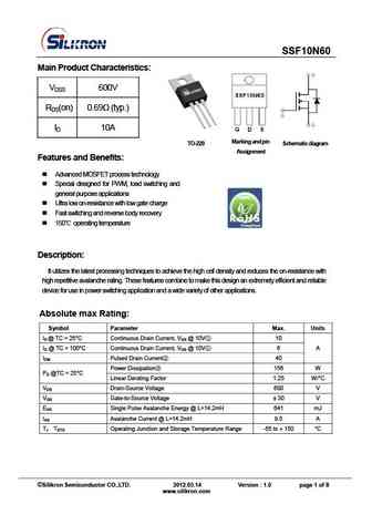
Pd ⓘ - Maximum Power Dissipation: 100 W
|Vds|ⓘ - Maximum Drain-Source Voltage: 800 V
|Vgs|ⓘ - Maximum Gate-Source Voltage: 30 V
|Id| ⓘ - Maximum Drain Current: 6.5 A
Tj ⓘ - Maximum Junction Temperature: 150 °C
Electrical Characteristics
tr ⓘ - Rise Time: 58 nS
Cossⓘ - Output Capacitance: 260 pF
RDSonⓘ - Maximum Drain-Source On-State Resistance: 0.95 Ohm
Package: TO3PF
📄📄 Copy
SSF10N80A substitution
- MOSFET ⓘ Cross-Reference Search
SSF10N80A datasheet
ssf10n80a.pdf
Advanced Power MOSFET FEATURES BVDSS = 800 V Avalanche Rugged Technology RDS(on) = 0.95 Rugged Gate Oxide Technology Lower Input Capacitance ID = 6.5 A Improved Gate Charge Extended Safe Operating Area Lower Leakage Current 25 A (Max.) @ VDS = 800V Low RDS(ON) 0.746 (Typ.) 1 2 3 1.Gate 2. Drain 3. Source Absolute Maximum Ratings Symbol Characteristic Val... See More ⇒
ssf10n60a.pdf
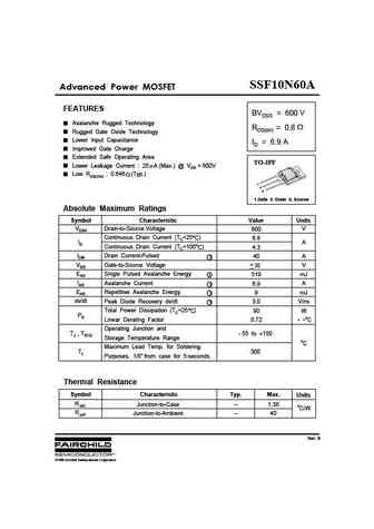
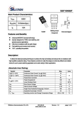
SSF10N60A Advanced Power MOSFET FEATURES BVDSS = 600 V Avalanche Rugged Technology RDS(on) = 0.8 Rugged Gate Oxide Technology Lower Input Capacitance ID = 6.9 A Improved Gate Charge Extended Safe Operating Area TO-3PF Lower Leakage Current 25 A (Max.) @ VDS = 600V Low RDS(ON) 0.646 (Typ.) 1 2 3 1.Gate 2. Drain 3. Source Absolute Maximum Ratings Symbol... See More ⇒
ssf10n90a.pdf
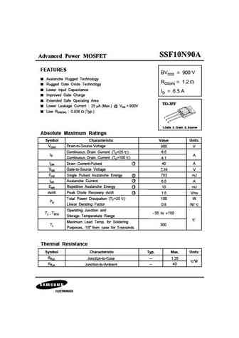
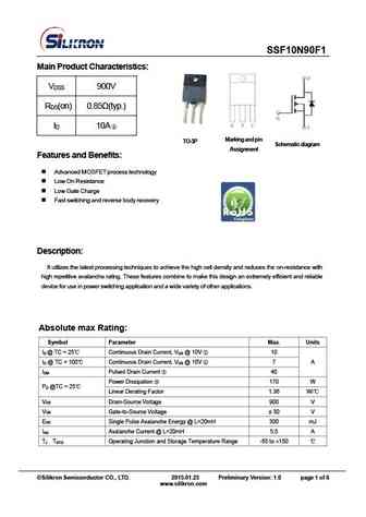
Advanced Power MOSFET FEATURES BVDSS = 900 V Avalanche Rugged Technology RDS(on) = 1.2 Rugged Gate Oxide Technology Lower Input Capacitance ID = 6.5 A Improved Gate Charge Extended Safe Operating Area Lower Leakage Current 25 A (Max.) @ VDS = 900V Low RDS(ON) 0.938 (Typ.) 1 2 3 1.Gate 2. Drain 3. Source Absolute Maximum Ratings Symbol Characteristic Valu... See More ⇒
Detailed specifications: SML80H14, SML80J25, SML80J28, SML80J44, SML80L27, SML80S13, SML80T27, SSF10N60A, 7N60, SSF10N90A, SSF17N60A, SSF22N50A, SSF25N40A, SSF45N20A, SSF4N80AS, SSF4N90AS, SSF5N80A
Keywords - SSF10N80A MOSFET specs
SSF10N80A cross reference
SSF10N80A equivalent finder
SSF10N80A pdf lookup
SSF10N80A substitution
SSF10N80A replacement
Can't find your MOSFET? Learn how to find a substitute transistor by analyzing voltage, current and package compatibility
History: IXTT30N50P | IRF9Z14L | IXTQ200N06P | MTA340N02KC3 | PDP0959 | UPA2727T1A | IRF9620PBF
🌐 : EN ES РУ
LIST
Last Update
MOSFET: BCD70N07A | BCD90N03 | BCD80N06 | T50N06 | H50N06 | BCD12N65 | BCT12N65 | BCD4N65 | BCT4N65 | BCD7N65
Popular searches
mj15023 | tip36c transistor | 2sc3320 | 2sc2078 | ac127 transistor | a42 transistor | bc547c | 2sa726
