50N06D Specs and Replacement
Type Designator: 50N06D
Type of Transistor: MOSFET
Type of Control Channel: N-Channel
Absolute Maximum Ratings
Pd ⓘ
- Maximum Power Dissipation: 100 W
|Vds|ⓘ - Maximum Drain-Source Voltage: 60 V
|Vgs|ⓘ - Maximum Gate-Source Voltage: 20 V
|Id| ⓘ - Maximum Drain Current: 50 A
Tj ⓘ - Maximum Junction Temperature: 150 °C
Electrical Characteristics
tr ⓘ - Rise Time: 380 nS
Cossⓘ -
Output Capacitance: 445 pF
RDSonⓘ - Maximum Drain-Source On-State Resistance: 0.0175 Ohm
Package: TO251
- MOSFET ⓘ Cross-Reference Search
50N06D datasheet
..1. Size:521K chongqing pingwei
50n06 50n06f 50n06b 50n06h 50n06g 50n06d.pdf 
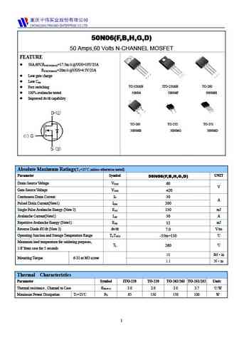
50N06(F,B,H,G,D) 50 Amps,60 Volts N-CHANNEL MOSFET FEATURE 50A,60V,R =17.5m @VGS=10V/25A DS(ON)MAX R =20m @VGS=4.5V/25A DS(ON)MAX Low gate charge Low C iss TO-220AB ITO-220AB TO-262 Fast switching 100% avalanche tested 50N06 50N06F 50N06H Improved dv/dt capability TO-263 TO-252 TO-251 50N06B 50N06G 50N06D Absolute Maximum Ratings(T =25 ,unless otherwi... See More ⇒
0.1. Size:837K blue-rocket-elect
brcs50n06dp.pdf
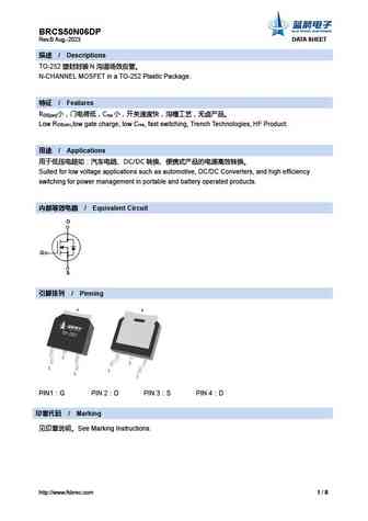
BRCS50N06DP Rev.B Aug.-2023 DATA SHEET / Descriptions TO-252 N N-CHANNEL MOSFET in a TO-252 Plastic Package. / Features R C DS(on) rss Low R ,low gate charge, low C , fast switching, Trench Technologies, HF Product. DS(on) rss / Applications ... See More ⇒
0.2. Size:336K first silicon
ftk50n06d.pdf
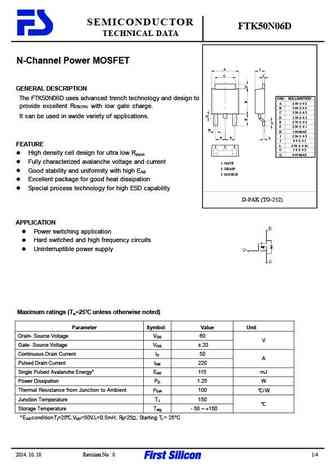
SEMICONDUCTOR FTK50N06D TECHNICAL DATA N-Channel Power MOSFET A I C J GENERAL DESCRIPTION The FTK50N06D uses advanced trench technology and design to DIM MILLIMETERS A 6 50 0 2 provide excellent RDS(ON) with low gate charge. B 5 60 0 2 C 5 20 0 2 It can be used in awide variety of applications. D 1 50 0 2 E 2 70 0 2 F 2 30 0 1 H H 1 00 MAX I 2 30 0... See More ⇒
0.3. Size:255K first silicon
ftk50n06dd.pdf
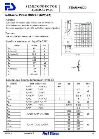
SEMICONDUCTOR FTK50N06DD TECHNICAL DATA N-Channel Power MOSFET (60V/50A) Purpose Suited for low voltage applications such as automotive, DC/DC Converters, and high efficiency switching for power management in portable and battery operated products Feature Low RDS(on),low gate charge,low Crss,fast switching. Absolute maximum ratings(Ta=25 ) Rating Symbol Unit V 60 V DSS ... See More ⇒
0.5. Size:738K feihonltd
fhp50n06 fhu50n06d fhd50n06d.pdf
N N-CHANNEL MOSFET FHP50N06/FHU50N06D/FHD50N06D MAIN CHARACTERISTICS FEATURES ID 50 A Low gate charge VDSS 60 V Crss ( 130pF) Low Crss (typical 130pF ) Rdson-typ @Vgs=10V 8.5m Fast switching Qg-typ 40nC 100% 100% avalanche tested dv/dt... See More ⇒
0.7. Size:101K sirectifier
sg50n06dt.pdf
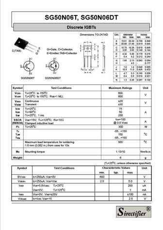
SG50N06T, SG50N06DT Discrete IGBTs Dimensions TO-247AD Dim. Millimeter Inches Min. Max. Min. Max. A 19.81 20.32 0.780 0.800 B 20.80 21.46 0.819 0.845 C 15.75 16.26 0.610 0.640 E G=Gate, C=Collector, D 3.55 3.65 0.140 0.144 C(TAB) C E=Emitter,TAB=Collector G E 4.32 5.49 0.170 0.216 F 5.4 6.2 0.212 0.244 G 1.65 2.13 0.065 0.084 H - 4.5 - 0.177 J 1.0 1.4 0.040 0.055 K 10.8 11.0 ... See More ⇒
0.8. Size:149K sirectifier
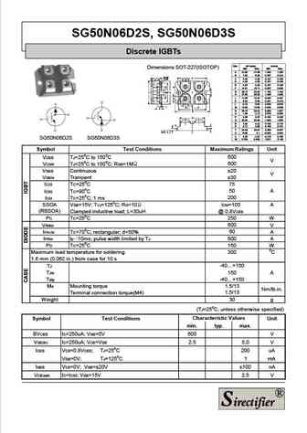
sg50n06d2s.pdf

SG50N06D2S, SG50N06D3S Discrete IGBTs Dim. Millimeter Inches Dimensions SOT-227(ISOTOP) Min. Max. Min. Max. A 31.50 31.88 1.240 1.255 B 7.80 8.20 0.307 0.323 C 4.09 4.29 0.161 0.169 D 4.09 4.29 0.161 0.169 E 4.09 4.29 0.161 0.169 F 14.91 15.11 0.587 0.595 G 30.12 30.30 1.186 1.193 H 37.80 38.20 1.489 1.505 J 11.68 12.22 0.460 0.481 K 8.92 9.60 0.351 0.378 L 0.76 0.84 0.030 0.033 ... See More ⇒
0.9. Size:149K sirectifier
sg50n06d3s.pdf
SG50N06D2S, SG50N06D3S Discrete IGBTs Dim. Millimeter Inches Dimensions SOT-227(ISOTOP) Min. Max. Min. Max. A 31.50 31.88 1.240 1.255 B 7.80 8.20 0.307 0.323 C 4.09 4.29 0.161 0.169 D 4.09 4.29 0.161 0.169 E 4.09 4.29 0.161 0.169 F 14.91 15.11 0.587 0.595 G 30.12 30.30 1.186 1.193 H 37.80 38.20 1.489 1.505 J 11.68 12.22 0.460 0.481 K 8.92 9.60 0.351 0.378 L 0.76 0.84 0.030 0.033 ... See More ⇒
0.10. Size:152K sirectifier
sg50n06ds.pdf
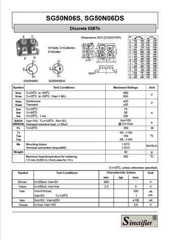
SG50N06S, SG50N06DS Discrete IGBTs C Dim. Millimeter Inches E Dimensions SOT-227(ISOTOP) Min. Max. Min. Max. A 31.50 31.88 1.240 1.255 B 7.80 8.20 0.307 0.323 C 4.09 4.29 0.161 0.169 D 4.09 4.29 0.161 0.169 E 4.09 4.29 0.161 0.169 G=Gate, C=Collector, F 14.91 15.11 0.587 0.595 G 30.12 30.30 1.186 1.193 E=Emitter H 37.80 38.20 1.489 1.505 J 11.68 12.22 0.460 0.481 K 8.92 9.60 0... See More ⇒
0.11. Size:955K slkor
sl50n06d sl50n06i.pdf
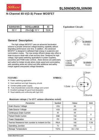
SL50N06D/SL50N06I N-Channel 60-V(D-S) Power MOSFET V(BR)DSS RDS(on)MAX ID Equivalent Circuit 60 V 20m @ 10 V 50A General Description 2 SL50N06D The high voltage MOSFET uses an advanced termination 3 scheme to provide enhanced voltage-blocking capability without degrading performance over time. In addition , this advanced MOSFET is designed to withstand high energy in avalanche ... See More ⇒
0.12. Size:499K convert
cs50n06f cs50n06p cs50n06u cs50n06d.pdf
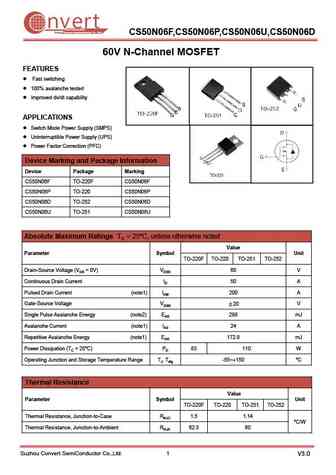
nvert Suzhou Convert Semiconductor Co ., Ltd. CS50N06F,CS50N06P,CS50N06U,CS50N06D 60V N-Channel MOSFET FEATURES Fast switching 100% avalanche tested Improved dv/dt capability APPLICATIONS Switch Mode Power Supply (SMPS) Uninterruptible Power Supply (UPS) Power Factor Correction (PFC) Device Marking and Package Information Device Package Marking CS50N06F TO-... See More ⇒
0.13. Size:2042K haolin elec
hd50n06d hu50n06d.pdf
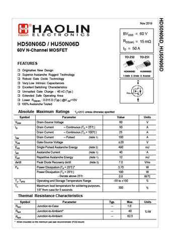
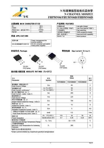
Nov 2019 BVDSS = 60 V RDS(on) = 15 m HD50N06D / HU50N06D ID = 50 A 60V N-Channel MOSFET TO-252 TO-251 FEATURES Originative New Design HD50N06D HU50N06D Superior Avalanche Rugged Technology 1.Gate 2. Drain 3. Source Robust Gate Oxide Technology Very Low Intrinsic Capacitances Excellent Switching Characteristics Unrivalled Gate Charge 40 nC (Typ.) ... See More ⇒
0.14. Size:988K cn vbsemi
hs50n06da.pdf
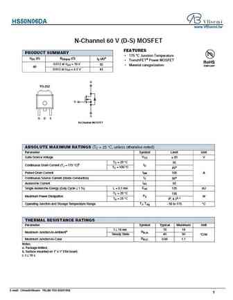
HS50N06DA www.VBsemi.tw N-Channel 60 V (D-S) MOSFET FEATURES PRODUCT SUMMARY 175 C Junction Temperature VDS (V) RDS(on) ( ) ID (A)a TrenchFET Power MOSFET 0.012 at VGS = 10 V 50 Material categorization 60 0.013 at VGS = 4.5 V 45 D TO-252 G S G D S N-Channel MOSFET ABSOLUTE MAXIMUM RATINGS (TC = 25 C, unless otherwise noted) Parameter Symbol Limit ... See More ⇒
0.15. Size:730K cn hmsemi
hm50n06d.pdf
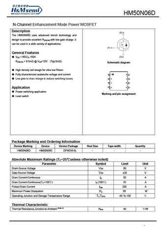
HM50N06D N-Channel Enhancement Mode Power MOSFET Description The HM50N06D uses advanced trench technology and design to provide excellent RDS(ON) with low gate charge. It can be used in a wide variety of applications. General Features VDS = 60V,ID =50A RDS(ON) ... See More ⇒
0.16. Size:590K cn hmsemi
hms150n06d.pdf
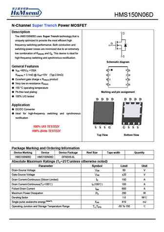
HMS150N06D N-Channel Super Trench Power MOSFET Description The HMS150N06D uses Super Trench technology that is uniquely optimized to provide the most efficient high frequency switching performance. Both conduction and switching power losses are minimized due to an extremely low combination of RDS(ON) and Qg. This device is ideal for high-frequency switching and synchronous recti... See More ⇒
0.17. Size:1036K cn minos
mdt50n06d.pdf
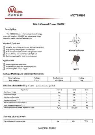
60V N-Channel Power MOSFE Description The MDT50N06 uses advanced trench technology to provide excellent RDS(ON), low gate charge. It can be used in a wide variety of applications. General Features V =60V, R ... See More ⇒
0.18. Size:2272K cn apm
ap50n06d.pdf
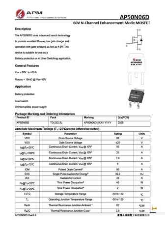
AP50N06D 60V N-Channel Enhancement Mode MOSFET Description The AP50N06D uses advanced trench technology to provide excellent R , low gate charge and DS(ON) operation with gate voltages as low as 4.5V. This device is suitable for use as a Battery protection or in other Switching application. General Features V = 60V I =50 A DS D R ... See More ⇒
0.19. Size:3648K cn apm
ap50n06df.pdf
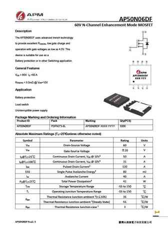
AP50N06DF 60V N-Channel Enhancement Mode MOSFET Description The AP50N06DF uses advanced trench technology to provide excellent R , low gate charge and DS(ON) operation with gate voltages as low as 4.5V. This device is suitable for use as a Battery protection or in other Switching application. General Features V = 60V I =50 A DS D R ... See More ⇒
Detailed specifications: 4N65F, 4N65B, 4N65H, 4N65G, 4N65D, 4N65TF, 50N06B, 50N06H, IRF3205, 5N65GS, 5N70GS, 7N60GS, 7N60DS, 7N60TF, 8N06G, 8N06D, M4N65TF
Keywords - 50N06D MOSFET specs
50N06D cross reference
50N06D equivalent finder
50N06D pdf lookup
50N06D substitution
50N06D replacement
Need a MOSFET replacement?
Our guide shows you how to find a perfect substitute by comparing key parameters and specs