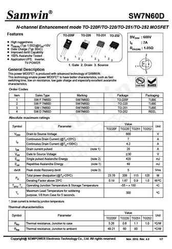
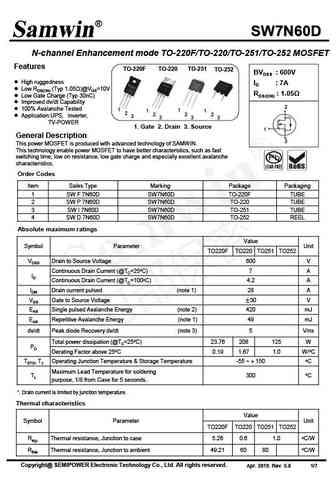
7N60DS Specs and Replacement
Type Designator: 7N60DS
Type of Transistor: MOSFET
Type of Control Channel: N-Channel
Absolute Maximum Ratings
Pd ⓘ - Maximum Power Dissipation: 63 W
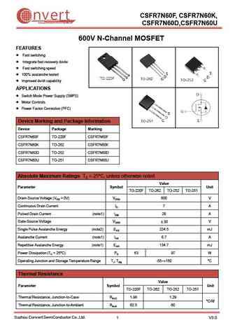
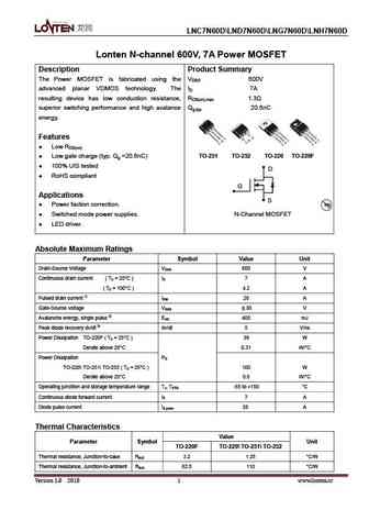
|Vds|ⓘ - Maximum Drain-Source Voltage: 600 V
|Vgs|ⓘ - Maximum Gate-Source Voltage: 20 V
|Id| ⓘ - Maximum Drain Current: 7 A
Tj ⓘ - Maximum Junction Temperature: 150 °C
Electrical Characteristics
tr ⓘ - Rise Time: 6.2 nS
Cossⓘ - Output Capacitance: 310 pF
RDSonⓘ - Maximum Drain-Source On-State Resistance: 0.58 Ohm
Package: TO251
7N60DS substitution
- MOSFET ⓘ Cross-Reference Search
7N60DS datasheet
7n60gs 7n60ds.pdf
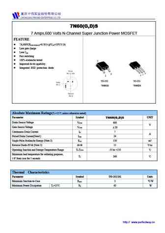
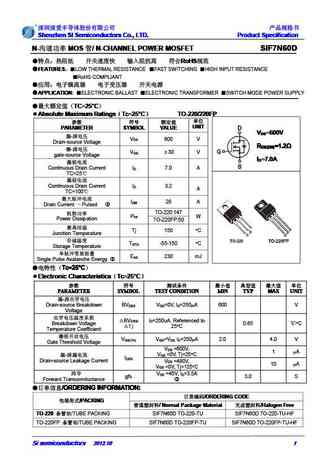
7N60(G,D)S 7 Amps,600 Volts N-Channel Super Junction Power MOSFET FEATURE 7A,600V,R =0.58 @V =10V/3.5A DS(ON)MAX GS Low gate charge Low C iss Fast switching 100% avalanche tested Improved dv/dt capability Integrated ESD protection diode TO-252 TO-251 7N60GS 7N60DS Absolute Maximum Ratings(T =25 ,unless otherwise noted) C Parameter Symbol UNIT 7N60... See More ⇒
stb37n60dm2ag.pdf
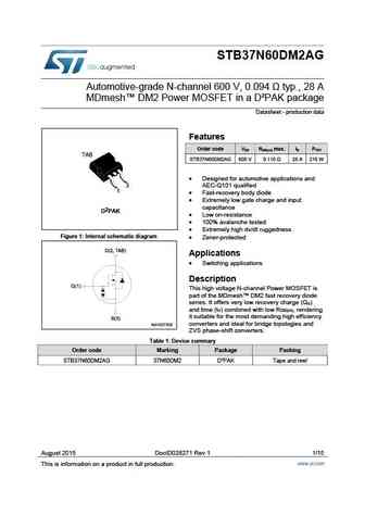
STB37N60DM2AG Automotive-grade N-channel 600 V, 0.094 typ., 28 A MDmesh DM2 Power MOSFET in a D PAK package Datasheet - production data Features Order code VDS RDS(on) max. ID PTOT TAB STB37N60DM2AG 600 V 0.110 28 A 210 W Designed for automotive applications and 3 AEC-Q101 qualified 1 Fast-recovery body diode Extremely low gate charge and input capa... See More ⇒
stw37n60dm2ag.pdf
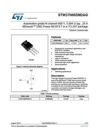
STW37N60DM2AG Automotive-grade N-channel 600 V, 0.094 typ., 28 A MDmesh DM2 Power MOSFET in a TO-247 package Datasheet - production data Features Order code VDS RDS(on) max. ID PTOT STW37N60DM2AG 600 V 0.110 28 A 210 W Designed for automotive applications and AEC-Q101 qualified 3 Fast-recovery body diode 2 Extremely low gate charge and input 1 capac... See More ⇒
sihp17n60d.pdf
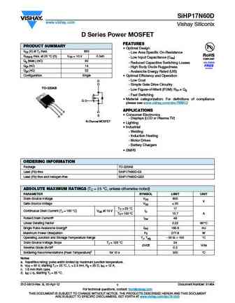
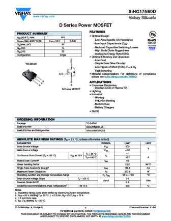
SiHP17N60D www.vishay.com Vishay Siliconix D Series Power MOSFET FEATURES PRODUCT SUMMARY Optimal Design VDS (V) at TJ max. 650 - Low Area Specific On-Resistance RDS(on) max. at 25 C ( ) VGS = 10 V 0.340 - Low Input Capacitance (Ciss) Qg (Max.) (nC) 90 - Reduced Capacitive Switching Losses Qgs (nC) 14 - High Body Diode Ruggedness Qgd (nC) 22 - Avalanche Energy Rated (UIS... See More ⇒
Detailed specifications: 4N65D, 4N65TF, 50N06B, 50N06H, 50N06D, 5N65GS, 5N70GS, 7N60GS, IRF540N, 7N60TF, 8N06G, 8N06D, M4N65TF, FS8205, FMD5N50E5, FKBA3004, FKBA3006
Keywords - 7N60DS MOSFET specs
7N60DS cross reference
7N60DS equivalent finder
7N60DS pdf lookup
7N60DS substitution
7N60DS replacement
Need a MOSFET replacement? Our guide shows you how to find a perfect substitute by comparing key parameters and specs
History: SSM3K335
🌐 : EN ES РУ

LIST
Last Update
MOSFET: AUB034N10 | AUB033N08BG | AUB026N085 | AUA062N08BG | AUA060N08AG | AUA056N08BGL | AUA039N10 | ASW80R290E | ASW65R120EFD | ASW65R110E
Popular searches
irfb3306 equivalent | irfp460 характеристики | k2837 datasheet | k389 transistor | mje15032g equivalent | nsd134 | 60r190p datasheet | cs30n20 datasheet