2N4392 Datasheet. Specs and Replacement
Type Designator: 2N4392 📄📄
Type of Transistor: JFET
Type of Control Channel: N-Channel
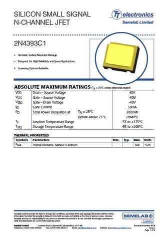
Absolute Maximum Ratings
Pd ⓘ - Maximum Power Dissipation: 1.8 W
|Vds|ⓘ - Maximum Drain-Source Voltage: 40 V
|Id| ⓘ - Maximum Drain Current: 0.15 A
Tj ⓘ - Maximum Junction Temperature: 150 °C
Electrical Characteristics
Cossⓘ - Output Capacitance: 14 pF
RDSonⓘ - Maximum Drain-Source On-State Resistance: 60 Ohm
Package: TO18
📄📄 Copy
2N4392 substitution
- MOSFET ⓘ Cross-Reference Search
2N4392 datasheet
2n4391 pn4391 sst4391 2n4392 pn4392 sst4392 2n4393 pn4393 sst4393.pdf
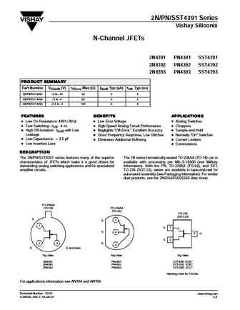
2N/PN/SST4391 Series Vishay Siliconix N-Channel JFETs 2N4391 PN4391 SST4391 2N4392 PN4392 SST4392 2N4393 PN4393 SST4393 PRODUCT SUMMARY Part Number VGS(off) (V) rDS(on) Max (W) ID(off) Typ (pA) tON Typ (ns) 2N/PN/SST4391 4 to 10 30 5 4 2N/PN/SST4392 2 to 5 60 5 4 2N/PN/SST4393 0.5 to 3 100 5 4 FEATURES BENEFITS APPLICATIONS D Low On-Resistance 4391... See More ⇒
2n4391 2n4392 2n4393.pdf
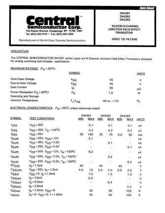
145 Adams Avenue, Hauppauge, NY 11788 USA Tel (631) 435-1110 Fax (631) 435-1824 TM Central Semiconductor Corp. 145 Adams Avenue Hauppauge, NY 11788 USA Tel (631) 435-1110 Fax (631) 435-1824 www.centralsemi.com ... See More ⇒
2n4392.pdf
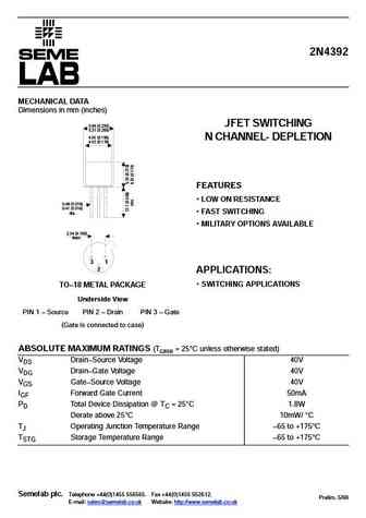
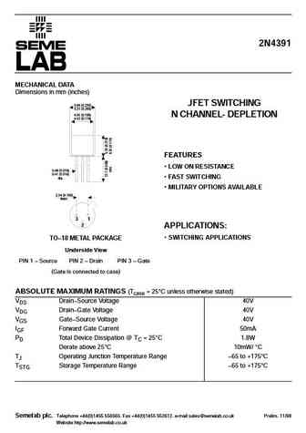
2N4392 MECHANICAL DATA Dimensions in mm (inches) JFET SWITCHING 5.84 (0.230) 5.31 (0.209) 4.95 (0.195) N CHANNEL- DEPLETION 4.52 (0.178) FEATURES LOW ON RESISTANCE 0.48 (0.019) 0.41 (0.016) FAST SWITCHING dia. MILITARY OPTIONS AVAILABLE 2.54 (0.100) Nom. 3 1 2 APPLICATIONS SWITCHING APPLICATIONS TO 18 METAL PACKAGE Underside View PIN 1 Source PIN 2... See More ⇒
2n4391 2n4392 2n4393 pn4391 pn4392 pn4393 sst4391 sst4392 sst4393.pdf
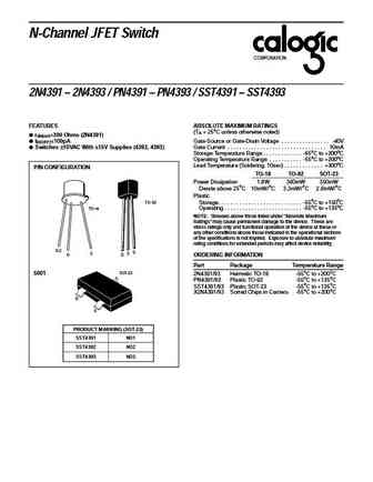
N-Channel JFET Switch CORPORATION 2N4391 2N4393 / PN4391 PN4393 / SST4391 SST4393 FEATURES ABSOLUTE MAXIMUM RATINGS (T = 25oC unless otherwise noted) A r ... See More ⇒

Detailed specifications: IRF540N, 2N4392CSM, 2N4393, 2N4393CSM, 2N4416, 2N5045, 2N5484, 2N5485, 2N5486
Keywords - 2N4392 MOSFET specs
2N4392 cross reference
2N4392 equivalent finder
2N4392 pdf lookup
2N4392 substitution
2N4392 replacement
Need a MOSFET replacement? Our guide shows you how to find a perfect substitute by comparing key parameters and specs
🌐 : EN ES РУ

LIST
Last Update
MOSFET: MSH100N045SA | MSD60P16 | MSD40P45 | MSB100N023 | MS60P03 | MS40P05AU | MS40P05 | MS40N05 | MS34P07 | MS34P01
Popular searches
bc547 transistor | bd139 | 2n4401 datasheet | irf640 | irf840 | irf740 | c945 transistor | irf640n