DMP610DL Specs and Replacement
Type Designator: DMP610DL
Type of Transistor: MOSFET
Type of Control Channel: P-Channel
Absolute Maximum Ratings
Pd ⓘ - Maximum Power Dissipation: 0.5 W
|Vds|ⓘ - Maximum Drain-Source Voltage: 60 V
|Vgs|ⓘ - Maximum Gate-Source Voltage: 30 V
|Id| ⓘ - Maximum Drain Current: 0.18 A
Tj ⓘ - Maximum Junction Temperature: 150 °C
Electrical Characteristics
tr ⓘ - Rise Time: 2.6 nS
Cossⓘ - Output Capacitance: 4.8 pF
RDSonⓘ - Maximum Drain-Source On-State Resistance: 10 Ohm
Package: SOT23
DMP610DL substitution
- MOSFET ⓘ Cross-Reference Search
DMP610DL datasheet
dmp610dl.pdf
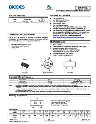
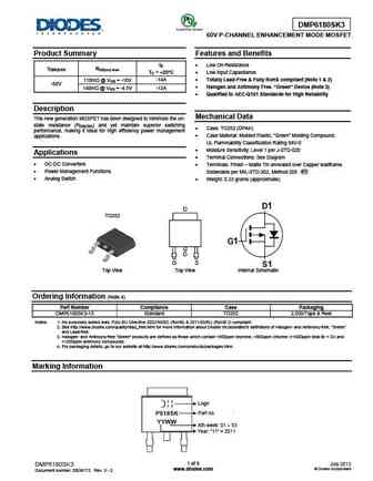
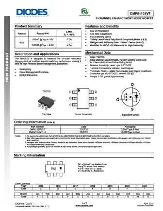
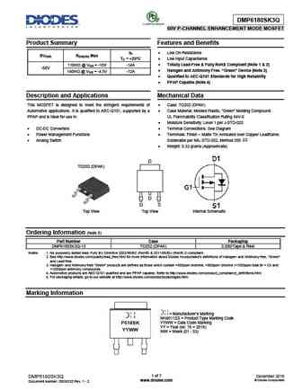
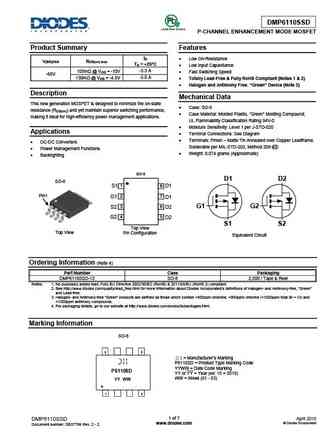
DMP610DL P-CHANNEL ENHANCEMENT MODE MOSFET Product Summary Features and Benefits Low On-Resistance I D BV R Max DSS DS(ON) Low Gate Threshold Voltage T = +25 C A -60V 10 @ V = -5V -180mA Low Input Capacitance GS Fast Switching Speed Low Input/Output Leakage Totally Lead-Free & Fully RoHS Compliant (Notes 1 & 2) Halogen and Antimony Fr... See More ⇒
dmp6185se.pdf
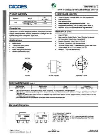
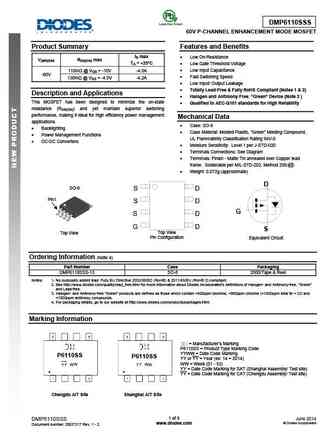
DMP6185SE 60V P-CHANNEL ENHANCEMENT MODE MOSFET Product Summary Features and Benefits 100% Unclamped Inductive Switch (UIS) test in production ID V(BR)DSS RDS(on) TA = +25 C Low on-resistance Fast switching speed 150m @ VGS= -10V -3A -60V Lead-Free Finish; RoHS compliant (Notes 1 & 2) 185m @ VGS= -4.5V -2.7A Halogen and Antimony Free. Green ... See More ⇒
dmp6185seq.pdf
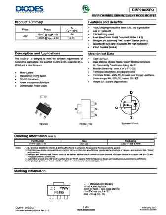
DMP6185SEQ 60V P-CHANNEL ENHANCEMENT MODE MOSFET Product Summary Features and Benefits ID 100% Unclamped Inductive Switch (UIS) test in production BVDSS RDS(on) TA = +25 C Low on-resistance Fast switching speed 150m @ VGS= -10V -3A -60V Lead-Free Finish; RoHS Compliant (Notes 1 & 2) 185m @ VGS= -4.5V -2.7A Halogen and Antimony Free. Green D... See More ⇒
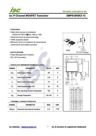
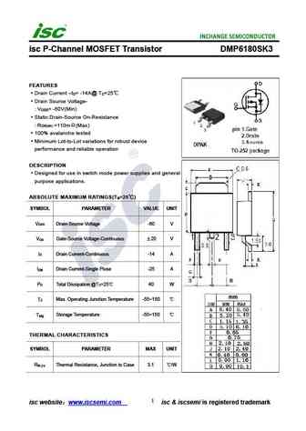
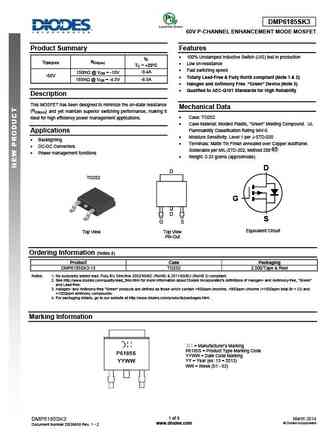
Detailed specifications: DMP3036SFV, DMP3098LQ, DMP3125L, DMP32D5SFB, DMP4013LFGQ, DMP4065SQ, DMP510DL, DMP6050SFG, 8205A, DMP6110SVT, DMP6180SK3Q, DMP6185SEQ, DMP6350S, DMPH6050SK3, DMPH6050SK3Q, DMT10H009LCG, DMT10H010LK3
Keywords - DMP610DL MOSFET specs
DMP610DL cross reference
DMP610DL equivalent finder
DMP610DL pdf lookup
DMP610DL substitution
DMP610DL replacement
Learn how to find the right MOSFET substitute. A guide to cross-reference, check specs and replace MOSFETs in your circuits.
History: DMTH4007LPS | DMT3002LPS
🌐 : EN ES РУ

LIST
Last Update
MOSFET: AUB034N10 | AUB033N08BG | AUB026N085 | AUA062N08BG | AUA060N08AG | AUA056N08BGL | AUA039N10 | ASW80R290E | ASW65R120EFD | ASW65R110E
Popular searches
svt20240nt | tip41c replacement | b772m transistor | mj15003g datasheet | irfp460n datasheet | mj15025g | ksa1381 replacement | m3056m mosfet