19N20 Specs and Replacement
Type Designator: 19N20
Type of Transistor: MOSFET
Type of Control Channel: N-Channel
Absolute Maximum Ratings
Pd ⓘ
- Maximum Power Dissipation: 80 W
|Vds|ⓘ - Maximum Drain-Source Voltage: 60 V
|Vgs|ⓘ - Maximum Gate-Source Voltage: 20 V
|Id| ⓘ - Maximum Drain Current: 19 A
Tj ⓘ - Maximum Junction Temperature: 175 °C
Electrical Characteristics
RDSonⓘ - Maximum Drain-Source On-State Resistance: 0.17 Ohm
Package: TO263
- MOSFET ⓘ Cross-Reference Search
19N20 datasheet
..1. Size:255K inchange semiconductor
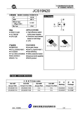
19n20.pdf 
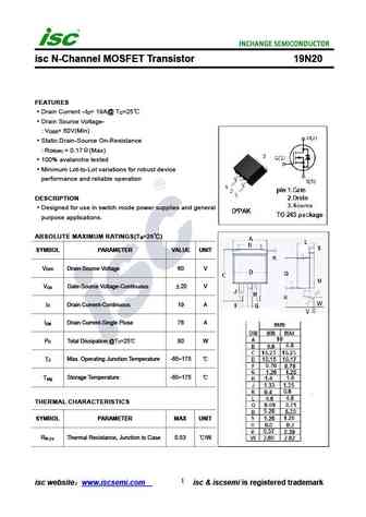
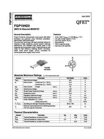
isc N-Channel MOSFET Transistor 19N20 FEATURES Drain Current I = 19A@ T =25 D C Drain Source Voltage- V = 60V(Min) DSS Static Drain-Source On-Resistance R = 0.17 (Max) DS(on) 100% avalanche tested Minimum Lot-to-Lot variations for robust device performance and reliable operation DESCRIPTION Designed for use in switch mode power supplies and general purpose ... See More ⇒
0.1. Size:61K st
stb19n20.pdf
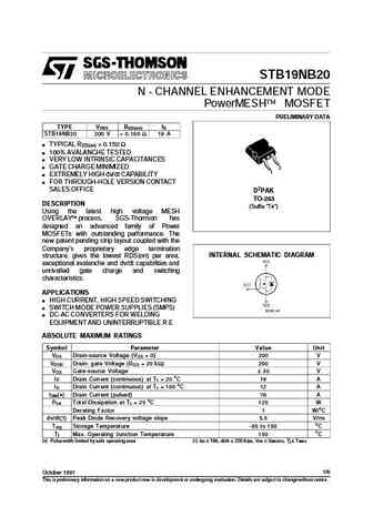
STB19NB20 N - CHANNEL ENHANCEMENT MODE PowerMESH MOSFET PRELIMINARY DATA TYPE V R I DSS DS(on) D STB19NB20 200 V ... See More ⇒
0.2. Size:686K fairchild semi
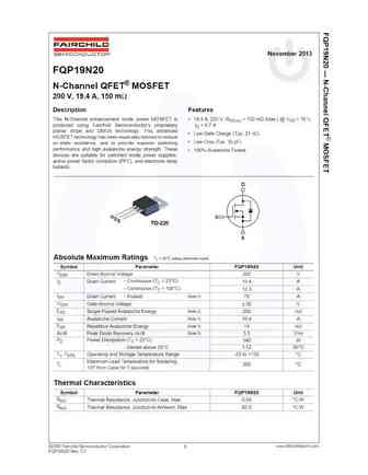
fqpf19n20t.pdf

April 2000 TM QFET QFET QFET QFET 200V N-ChanneI MOSFET GeneraI Description Features These N-Channel enhancement mode power field effect 11.8A, 200V, RDS(on) = 0.15 @VGS = 10 V transistors are produced using Fairchild s proprietary, Low gate charge ( typical 31 nC) planar stripe, DMOS technology. Low Crss ( typical 30 pF) This advanced technology has be... See More ⇒
0.3. Size:731K fairchild semi
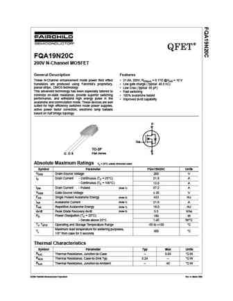
fqa19n20l.pdf
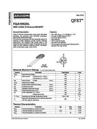
May 2000 TM QFET QFET QFET QFET 200V LOGIC N-ChanneI MOSFET GeneraI Description Features These N-Channel enhancement mode power field effect 25A, 200V, RDS(on) = 0.14 @VGS = 10 V transistors are produced using Fairchild s proprietary, Low gate charge ( typical 27 nC) planar stripe, DMOS technology. Low Crss ( typical 30 pF) This advanced technology has b... See More ⇒
0.4. Size:1168K fairchild semi
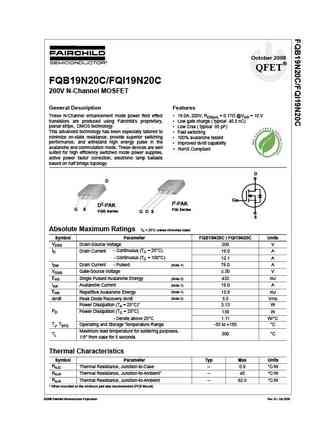
fqp19n20ctstu fqp19n20c fqpf19n20c fqpf19n20cydtu.pdf
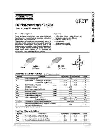
QFET FQP19N20C/FQPF19N20C 200V N-Channel MOSFET General Description Features These N-Channel enhancement mode power field effect 19.0A, 200V, RDS(on) = 0.17 @VGS = 10 V transistors are produced using Fairchild s proprietary, Low gate charge ( typical 40.5 nC) planar stripe, DMOS technology. Low Crss ( typical 85 pF) This advanced technology has been especially tailo... See More ⇒
0.5. Size:831K fairchild semi
fqb19n20tm fqb19n20 fqi19n20 fqi19n20tu.pdf
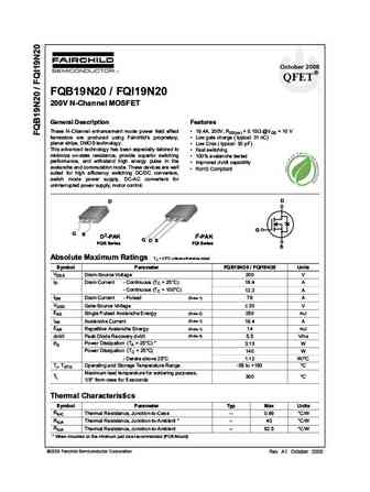
October 2008 QFET FQB19N20 / FQI19N20 200V N-ChanneI MOSFET GeneraI Description Features These N-Channel enhancement mode power field effect 19.4A, 200V, RDS(on) = 0.15 @VGS = 10 V transistors are produced using Fairchild s proprietary, Low gate charge ( typical 31 nC) planar stripe, DMOS technology. Low Crss ( typical 30 pF) This advanced technology has been espec... See More ⇒
0.6. Size:839K fairchild semi
fqb19n20ltm fqb19n20l fqi19n20l.pdf
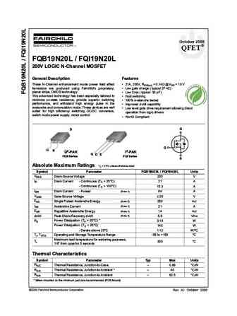
October 2008 QFET FQB19N20L / FQI19N20L 200V LOGIC N-ChanneI MOSFET GeneraI Description Features These N-Channel enhancement mode power field effect 21A, 200V, RDS(on) = 0.14 @VGS = 10 V transistors are produced using Fairchild s proprietary, Low gate charge ( typical 27 nC) planar stripe, DMOS technology. Low Crss ( typical 30 pF) This advanced technology has been ... See More ⇒
0.7. Size:722K fairchild semi
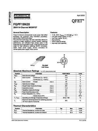
fqp19n20l.pdf

May 2000 TM QFET QFET QFET QFET 200V LOGIC N-ChanneI MOSFET GeneraI Description Features These N-Channel enhancement mode power field effect 21A, 200V, RDS(on) = 0.14 @VGS = 10 V transistors are produced using Fairchild s proprietary, Low gate charge ( typical 27 nC) planar stripe, DMOS technology. Low Crss ( typical 30 pF) This advanced technology has b... See More ⇒
0.8. Size:868K fairchild semi
fqa19n20c.pdf
QFET FQA19N20C 200V N-Channel MOSFET General Description Features These N-Channel enhancement mode power field effect 21.8A, 200V, RDS(on) = 0.17 @VGS = 10 V transistors are produced using Fairchild s proprietary, Low gate charge ( typical 40.5 nC) planar stripe, DMOS technology. Low Crss ( typical 85 pF) This advanced technology has been especially tailored to ... See More ⇒
0.9. Size:712K fairchild semi
fqaf19n20l.pdf
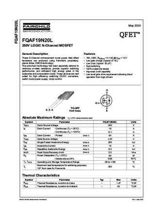
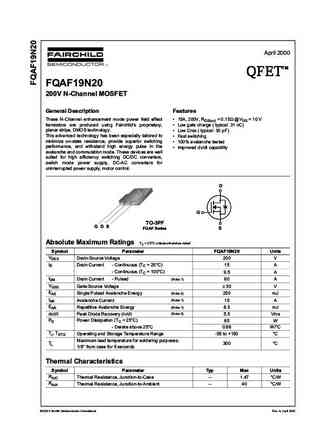
May 2000 TM QFET QFET QFET QFET 200V LOGIC N-ChanneI MOSFET GeneraI Description Features These N-Channel enhancement mode power field effect 16A, 200V, RDS(on) = 0.14 @VGS = 10 V transistors are produced using Fairchild s proprietary, Low gate charge ( typical 27 nC) planar stripe, DMOS technology. Low Crss ( typical 30 pF) This advanced technology has ... See More ⇒
0.10. Size:691K fairchild semi
fqpf19n20.pdf
April 2000 TM QFET QFET QFET QFET 200V N-ChanneI MOSFET GeneraI Description Features These N-Channel enhancement mode power field effect 11.8A, 200V, RDS(on) = 0.15 @VGS = 10 V transistors are produced using Fairchild s proprietary, Low gate charge ( typical 31 nC) planar stripe, DMOS technology. Low Crss ( typical 30 pF) This advanced technology has be... See More ⇒
0.11. Size:1167K fairchild semi
fqb19n20ctm fqb19n20c fqi19n20c fqi19n20ctu.pdf
October 2008 QFET FQB19N20C/FQI19N20C 200V N-Channel MOSFET General Description Features These N-Channel enhancement mode power field effect 19.0A, 200V, RDS(on) = 0.17 @VGS = 10 V transistors are produced using Fairchild s proprietary, Low gate charge ( typical 40.5 nC) planar stripe, DMOS technology. Low Crss ( typical 85 pF) This advanced technology has been espec... See More ⇒
0.12. Size:705K fairchild semi
fqp19n20.pdf
April 2000 TM QFET QFET QFET QFET 200V N-ChanneI MOSFET GeneraI Description Features These N-Channel enhancement mode power field effect 19.4A, 200V, RDS(on) = 0.15 @VGS = 10 V transistors are produced using Fairchild s proprietary, Low gate charge ( typical 31 nC) planar stripe, DMOS technology. Low Crss ( typical 30 pF) This advanced technology has bee... See More ⇒
0.13. Size:688K fairchild semi
fqaf19n20.pdf
April 2000 TM QFET QFET QFET QFET 200V N-ChanneI MOSFET GeneraI Description Features These N-Channel enhancement mode power field effect 15A, 200V, RDS(on) = 0.15 @VGS = 10 V transistors are produced using Fairchild s proprietary, Low gate charge ( typical 31 nC) planar stripe, DMOS technology. Low Crss ( typical 30 pF) This advanced technology has been... See More ⇒
0.14. Size:161K vishay
sud19n20-90.pdf
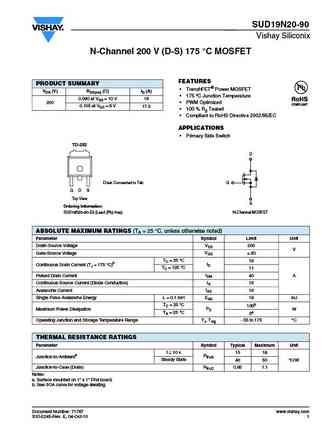
SUD19N20-90 Vishay Siliconix N-Channel 200 V (D-S) 175 C MOSFET FEATURES PRODUCT SUMMARY TrenchFET Power MOSFET VDS (V) RDS(on) ( )ID (A) 175 C Junction Temperature 0.090 at VGS = 10 V 19 PWM Optimized 200 0.105 at VGS = 6 V 17.5 100 % Rg Tested Compliant to RoHS Directive 2002/95/EC APPLICATIONS Primary Side Switch TO-252 D Drain Co... See More ⇒
0.15. Size:1047K onsemi
fqb19n20c.pdf

Is Now Part of To learn more about ON Semiconductor, please visit our website at www.onsemi.com Please note As part of the Fairchild Semiconductor integration, some of the Fairchild orderable part numbers will need to change in order to meet ON Semiconductor s system requirements. Since the ON Semiconductor product management systems do not have the ability to manage part nomenclatur... See More ⇒
0.16. Size:1000K onsemi
fqb19n20.pdf

Is Now Part of To learn more about ON Semiconductor, please visit our website at www.onsemi.com Please note As part of the Fairchild Semiconductor integration, some of the Fairchild orderable part numbers will need to change in order to meet ON Semiconductor s system requirements. Since the ON Semiconductor product management systems do not have the ability to manage part nomenclatur... See More ⇒
0.17. Size:789K onsemi
fqp19n20c fqpf19n20c.pdf

Is Now Part of To learn more about ON Semiconductor, please visit our website at www.onsemi.com Please note As part of the Fairchild Semiconductor integration, some of the Fairchild orderable part numbers will need to change in order to meet ON Semiconductor s system requirements. Since the ON Semiconductor product management systems do not have the ability to manage part nomenclatur... See More ⇒
0.18. Size:1034K onsemi
fqb19n20l.pdf

Is Now Part of To learn more about ON Semiconductor, please visit our website at www.onsemi.com Please note As part of the Fairchild Semiconductor integration, some of the Fairchild orderable part numbers will need to change in order to meet ON Semiconductor s system requirements. Since the ON Semiconductor product management systems do not have the ability to manage part nomenclatur... See More ⇒
0.20. Size:83K taiwansemi
tsm19n20cp.pdf
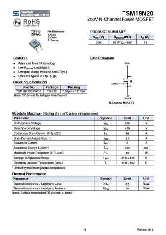
TSM19N20 200V N-Channel Power MOSFET TO-252 Pin Definition PRODUCT SUMMARY 1. Gate (DPAK) VDS (V) RDS(on)(m ) ID (A) 2. Drain 3. Source 200 92 @ VGS =10V 18 Features Block Diagram Advanced Trench Technology Low RDS(ON) 92m (Max.) Low gate charge typical @ 55nC (Typ.) Low Crss typical @ 73pF (Typ.) Ordering Information Part No. Package Pa... See More ⇒
0.21. Size:556K kec
kf19n20d.pdf
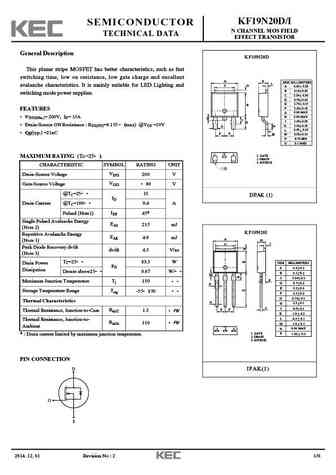
KF19N20D/I SEMICONDUCTOR N CHANNEL MOS FIELD TECHNICAL DATA EFFECT TRANSISTOR General Description KF19N20D This planar stripe MOSFET has better characteristics, such as fast switching time, low on resistance, low gate charge and excellent A K DIM MILLIMETERS L avalanche characteristics. It is mainly suitable for LED Lighting and C D _ A 6.60 + 0.20 _ B 6.10 + 0.20 switching mo... See More ⇒
0.22. Size:497K kec
khb019n20p1 f1 f2.pdf

KHB019N20P1/F1/F2 SEMICONDUCTOR N CHANNEL MOS FIELD TECHNICAL DATA EFFECT TRANSISTOR General Description KHB019N20P1 A O This planar stripe MOSFET has better characteristics, such as fast C F switching time, low on resistance, low gate charge and excellent E DIM MILLIMETERS G _ A 9.9 + 0.2 avalanche characteristics. It is mainly suitable for DC/DC converters B B 15.95 MAX Q ... See More ⇒
0.23. Size:541K kec
kf19n20f.pdf
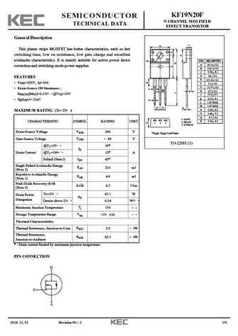
KF19N20F SEMICONDUCTOR N CHANNEL MOS FIELD TECHNICAL DATA EFFECT TRANSISTOR General Description C A This planar stripe MOSFET has better characteristics, such as fast switching time, low on resistance, low gate charge and excellent avalanche characteristics. It is mainly suitable for active power factor E DIM MILLIMETERS _ A 10.16 0.2 + correction and switching mode power suppli... See More ⇒
0.24. Size:90K kec
khb019n20f2 khb019n20p1.pdf
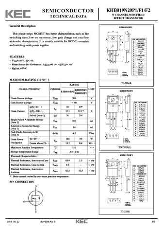
KHB019N20P1/F1/F2 SEMICONDUCTOR N CHANNEL MOS FIELD TECHNICAL DATA EFFECT TRANSISTOR General Description KHB019N20P1 A O This planar stripe MOSFET has better characteristics, such as fast C F switching time, low on resistance, low gate charge and excellent E DIM MILLIMETERS G _ A 9.9 + 0.2 avalanche characteristics. It is mainly suitable for DC/DC converters B B 15.95 MAX Q ... See More ⇒
0.26. Size:5069K first semi
fir19n20lg.pdf
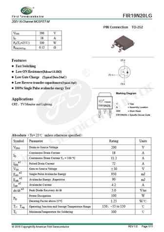
FIR19N20LG 200V N-Channel MOSFET-M PIN Connection TO-252 VDSS 200 V ID 18 A PD(TC=25 ) 100 W RDS(ON)Typ 0.12 Features Fast Switching Low ON Resistance(Rdson 0.18 ) ) Low Gate Charge (Typical Data 24nC Low Reverse transfer capacitances(Typical 25pF) 100% Single Pulse avalanche energy Test Marking Diagram Applications YAWW Y = Year CRT TV/Monitor and... See More ⇒
Detailed specifications: DMTH6009LK3Q, DMTH6010LK3, DMTH6010LPSQ, DMTH6016LSD, DMTH8003SPS, DMTH8012LPSW, ZXMP10A13FQ, ZXMS6005DGQ-13, 75N75, DMG10N60SCT, DMG3N60SJ3, DMG4N60SCT, DMG4N60SJ3, DMG4N60SK3, DMG7N65SCT, DMG7N65SCTI, DMG7N65SJ3
Keywords - 19N20 MOSFET specs
19N20 cross reference
19N20 equivalent finder
19N20 pdf lookup
19N20 substitution
19N20 replacement
Need a MOSFET replacement?
Our guide shows you how to find a perfect substitute by comparing key parameters and specs