DMG4N60SCT Specs and Replacement
Type Designator: DMG4N60SCT
Type of Transistor: MOSFET
Type of Control Channel: N-Channel
Absolute Maximum Ratings
Pd ⓘ - Maximum Power Dissipation: 113 W
|Vds|ⓘ - Maximum Drain-Source Voltage: 600 V
|Vgs|ⓘ - Maximum Gate-Source Voltage: 30 V
|Id| ⓘ - Maximum Drain Current: 4.5 A
Tj ⓘ - Maximum Junction Temperature: 150 °C
Electrical Characteristics
tr ⓘ - Rise Time: 34 nS
Cossⓘ - Output Capacitance: 47 pF
RDSonⓘ - Maximum Drain-Source On-State Resistance: 2.5 Ohm
Package: TO220AB
DMG4N60SCT substitution
- MOSFET ⓘ Cross-Reference Search
DMG4N60SCT datasheet
dmg4n60sct.pdf
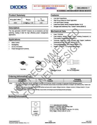
NOT RECOMMENDED FOR NEW DESIGN USE DMG3N60SCT DMG4N60SCT N-CHANNEL ENHANCEMENT MODE MOSFET Product Summary Features Low Input Capacitance ID BVDSS (@ TJ Max) RDS(ON) High BVDSS Rating for Power Application TC = +25 C Low Input/Output Leakage 650V 2.5 @VGS = 10V 4.5A Lead-Free Finish; RoHS Compliant (Notes 1 & 2) Halogen and Antimony Free. Gre... See More ⇒
dmg4n60sct.pdf
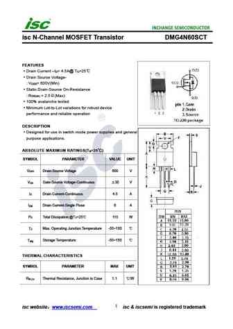
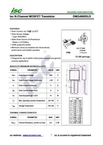
isc N-Channel MOSFET Transistor DMG4N60SCT FEATURES Drain Current I = 4.5A@ T =25 D C Drain Source Voltage- V = 600V(Min) DSS Static Drain-Source On-Resistance R = 2.5 (Max) DS(on) 100% avalanche tested Minimum Lot-to-Lot variations for robust device performance and reliable operation DESCRIPTION Designed for use in switch mode power supplies and general pu... See More ⇒
dmg4n60sj3.pdf
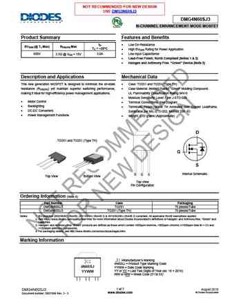
NOT RECOMMENDED FOR NEW DESIGN USE DMG3N60SJ3 DMG4N60SJ3 N-CHANNEL ENHANCEMENT MODE MOSFET Product Summary Features and Benefits ID Low On-Resistance BVDSS (@ TJ Max) RDS(ON) Max TC = +25 C High BVDSS Rating for Power Application 650V 3.0A Low Input Capacitance 2.5 @ VGS = 10V Lead-Free Finish; RoHS Compliant (Notes 1 & 2) Halogen and Antimony F... See More ⇒
dmg4n60sk3.pdf
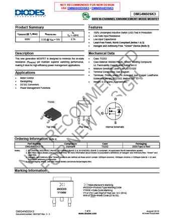
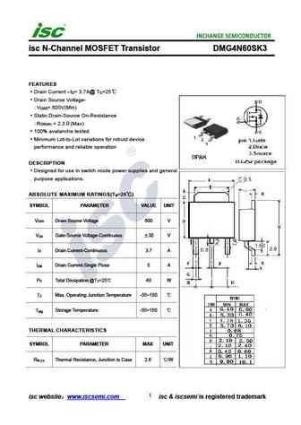
NOT RECOMMENDED FOR NEW DESIGN USE DMN60H3D5SK3 / DMN60H4D5SK3 DMG4N60SK3 600V N-CHANNEL ENHANCEMENT MODE MOSFET Product Summary Features ID 100% Unclamped Inductive Switch (UIS) Test in Production V(BR)DSS (@ TJ Max) RDS(ON) Max TC = +25 C Low Gate Input Resistance 650V 3.7A Low Input Capacitance 2.3 @ VGS = 10V Lead-Free Finish; RoHS Compliant (Note... See More ⇒
Detailed specifications: DMTH6016LSD, DMTH8003SPS, DMTH8012LPSW, ZXMP10A13FQ, ZXMS6005DGQ-13, 19N20, DMG10N60SCT, DMG3N60SJ3, STP65NF06, DMG4N60SJ3, DMG4N60SK3, DMG7N65SCT, DMG7N65SCTI, DMG7N65SJ3, DMG8N65SCT, DMJ70H1D0SV3, DMJ70H1D3SH3
Keywords - DMG4N60SCT MOSFET specs
DMG4N60SCT cross reference
DMG4N60SCT equivalent finder
DMG4N60SCT pdf lookup
DMG4N60SCT substitution
DMG4N60SCT replacement
Learn how to find the right MOSFET substitute. A guide to cross-reference, check specs and replace MOSFETs in your circuits.
🌐 : EN ES РУ

LIST
Last Update
MOSFET: AUB034N10 | AUB033N08BG | AUB026N085 | AUA062N08BG | AUA060N08AG | AUA056N08BGL | AUA039N10 | ASW80R290E | ASW65R120EFD | ASW65R110E
Popular searches
Популярные запросы | irfz44n | irf3205 | irfz44n datasheet | 2n4401 | bc547 transistor | bd139 | 2n4401 datasheet