FIR10N65FG Specs and Replacement
Type Designator: FIR10N65FG
Type of Transistor: MOSFET
Type of Control Channel: N-Channel
Absolute Maximum Ratings
Pd ⓘ - Maximum Power Dissipation: 50 W
|Vds|ⓘ - Maximum Drain-Source Voltage: 650 V
|Vgs|ⓘ - Maximum Gate-Source Voltage: 30 V
|Id| ⓘ - Maximum Drain Current: 10 A
Tj ⓘ - Maximum Junction Temperature: 150 °C
Electrical Characteristics
tr ⓘ - Rise Time: 73.67 nS
Cossⓘ - Output Capacitance: 128 pF
RDSonⓘ - Maximum Drain-Source On-State Resistance: 1 Ohm
Package: TO220F
FIR10N65FG substitution
- MOSFET ⓘ Cross-Reference Search
FIR10N65FG datasheet
fir10n65fg.pdf
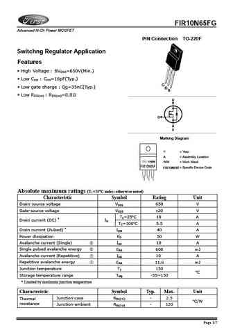
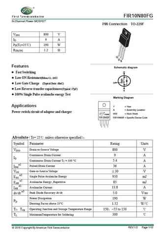
FIR10N65FG Advanced N-Ch Power MOSFET PIN Connection TO-220F Switchng Regulator Application Features High Voltage BVDSS=650V(Min.) Low Crss Crss=16pF(Typ.) G Low gate charge Qg=35nC(Typ.) D S Low RDS(on) RDS(on)=0.8 D G S Marking Diagram Y = Year A = Assembly Location YAWW WW = Work Week FIR10N65F FIR10N65F = Specific Device Code Absolu... See More ⇒
fir10n60fg.pdf
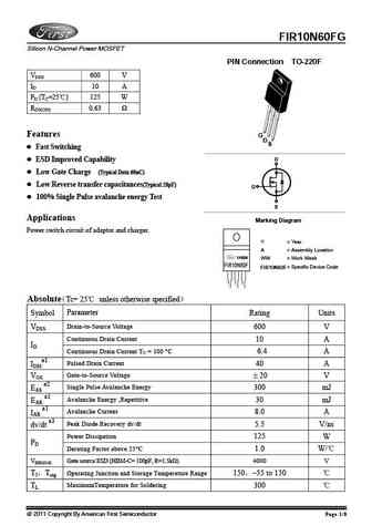
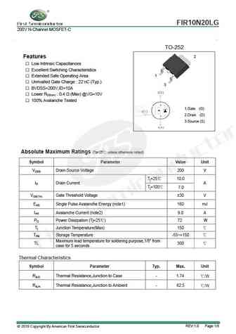
FIR10N60FG Silicon N-Channel Power MOSFET PIN Connection TO-220F VDSS 600 V ID 10 A PD (TC=25 ) 125 W RDS(ON) 0.63 Features G D S Fast Switching ESD Improved Capability D Low Gate Charge (Typical Data 60nC) Low Reverse transfer capacitances(Typical 28pF) G 100% Single Pulse avalanche energy Test S Applications Marking Diagram Power switch circuit of adap... See More ⇒
fir10n50fg.pdf
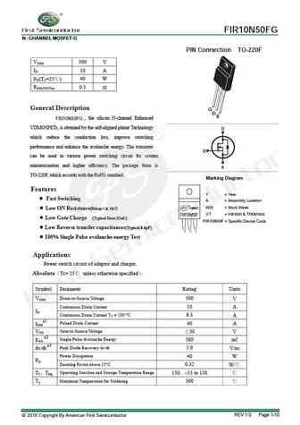
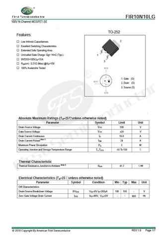
FIR10N50FG N - CHANNEL MOSFET-G PIN Connection TO-220F VDSS 500 V ID 10 A PD(TC=25 ) 40 W RDS(ON)Typ 0.5 General Description G D S , the silicon N-channel Enhanced FIR10N50FG VDMOSFETs, is obtained by the self-aligned planar Technology D which reduce the conduction loss, improve switching performance and enhance the avalanche energy. The transistor G can be... See More ⇒
fir10n70fg.pdf
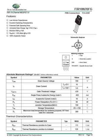
FIR10N70FG 700V N-Channel MOSFET-G PIN Connection TO-220F Features Low Intrinsic Capacitances. Excellent Switching Characteristics. Extended Safe Operating Area. Unrivalled Gate Charge Qg= 37nC (Typ.). BVDSS=700V,ID=10A G DS RDS(on) 1.0 (Max) @VG=10V 100% Avalanche Tested g Schematic dia ram D G S Marking Diagram Y = Year A = Assembly Locati... See More ⇒
Detailed specifications: EV3400, EV3401, EV3404, EV3407, EV3415, EY4409, GM4953, FIR10N60FG, IRF520, FIR12N60FG, FIR12N65FG, FIR20N65AFG, FIR2N60ALG, FIR2N65ABPG, FIR4N60BPG, FIR4N60FG, FIR4N60LG
Keywords - FIR10N65FG MOSFET specs
FIR10N65FG cross reference
FIR10N65FG equivalent finder
FIR10N65FG pdf lookup
FIR10N65FG substitution
FIR10N65FG replacement
Can't find your MOSFET? Learn how to find a substitute transistor by analyzing voltage, current and package compatibility
🌐 : EN ES РУ

LIST
Last Update
MOSFET: AUB062N08BG | AUB060N08AG | AUB056N10 | AUB056N08BGL | AUB050N085 | AUB050N055 | AUB045N12 | AUB045N10BT | AUB039N10 | AUB034N10
Popular searches
irf840 datasheet | ge10001 | irf830 | irfp450 | mj21193 | s9014 transistor | bc547 transistor datasheet | c945 datasheet