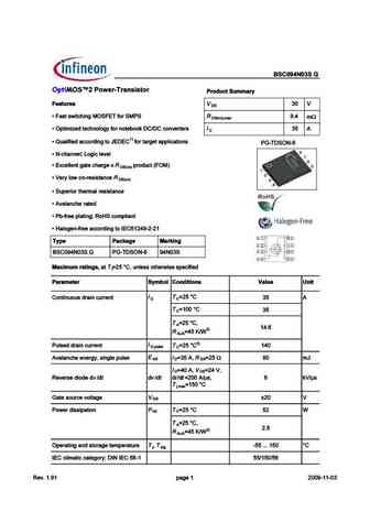
BSC096N10LS5 Specs and Replacement
Type Designator: BSC096N10LS5
Type of Transistor: MOSFET
Type of Control Channel: N-Channel
Absolute Maximum Ratings
Pd ⓘ
- Maximum Power Dissipation: 3 W
|Vds|ⓘ - Maximum Drain-Source Voltage: 100 V
|Vgs|ⓘ - Maximum Gate-Source Voltage: 20 V
|Id| ⓘ - Maximum Drain Current: 14 A
Tj ⓘ - Maximum Junction Temperature: 175 °C
Electrical Characteristics
tr ⓘ - Rise Time: 3.5 nS
Cossⓘ -
Output Capacitance: 250 pF
RDSonⓘ - Maximum Drain-Source On-State Resistance: 0.0096 Ohm
Package: SUPERSO8
BSC096N10LS5 substitution
- MOSFET ⓘ Cross-Reference Search
BSC096N10LS5 datasheet
..1. Size:1085K infineon
bsc096n10ls5.pdf 
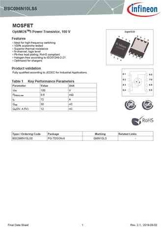
BSC096N10LS5 MOSFET SuperSO8 OptiMOSTM5 Power-Transistor, 100 V 5 8 6 7 Features 7 6 8 5 Ideal for high-frequency switching 100% avalanche tested Superior thermal resistance N-channel, logic level 4 Pb-free lead plating; RoHS compliant 1 3 2 2 Halogen-free according to IEC61249-2-21 3 1 4 Optimized for chargers Product validation Fully quali... See More ⇒
9.1. Size:816K infineon
bsc0902ns.pdf
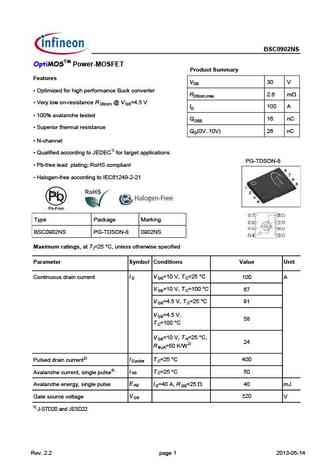
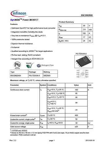
BSC0902NS OptiMOSTM Power-MOSFET Product Summary Features VDS 30 V Optimized for high performance Buck converter RDS(on),max 2.6 mW Very low on-resistance R @ V =4.5 V DS(on) GS ID 100 A 100% avalanche tested QOSS 16 nC Superior thermal resistance QG(0V..10V) 26 nC N-channel Qualified according to JEDEC1) for target applications PG-TDSON-8 ... See More ⇒
9.2. Size:521K infineon
bsc090n03lsg.pdf
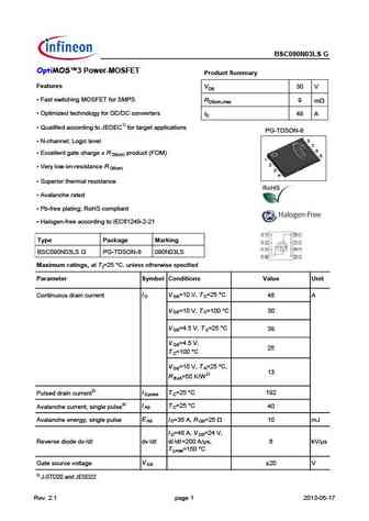
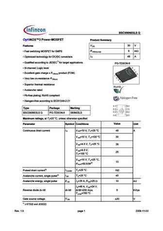
BSC090N03LS G OptiMOS 3 Power-MOSFET Product Summary Features VDS 30 V Fast switching MOSFET for SMPS RDS(on),max 9 mW Optimized technology for DC/DC converters ID 48 A Qualified according to JEDEC1) for target applications PG-TDSON-8 N-channel; Logic level Excellent gate charge x R product (FOM) DS(on) Very low on-resistance R DS(on) Superio... See More ⇒
9.3. Size:690K infineon
bsc0923ndi.pdf
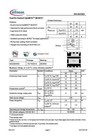
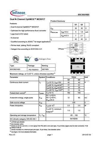
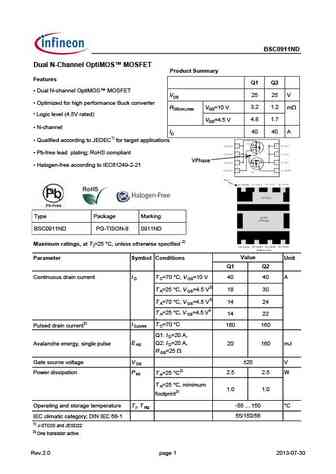
BSC0923NDI Dual N-Channel OptiMOS MOSFET Product Summary Features Q1 Q2 Dual N-channel OptiMOS MOSFET VDS 30 30 V Optimized for high performance Buck converter RDS(on),max VGS=10 V 5 2.8 mW Logic level (4.5V rated) VGS=4.5 V 7 3.7 100% avalanche tested ID 40 40 A Qualified according to JEDEC1) for target applications Pb-free lead plating; R... See More ⇒
9.4. Size:586K infineon
bsc0925nd.pdf
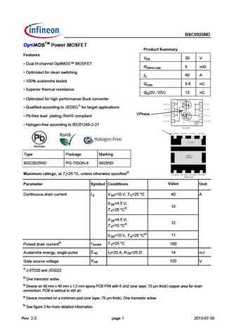
BSC0925ND OptiMOSTM Power-MOSFET Product Summary Features VDS 30 V Dual N-channel OptiMOS MOSFET RDS(on),max 5 mW Optimized for clean switching ID 40 A 100% avalanche tested QOSS 8.6 nC Superior thermal resistance QG(0V..10V) 13 nC Optimized for high performance Buck converter Qualified according to JEDEC1) for target applications VPhase ... See More ⇒
9.5. Size:520K infineon
bsc093n04lsg.pdf
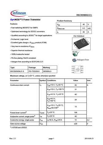
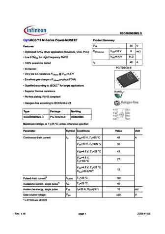
BSC093N04LS G OptiMOS 3 Power-Transistor Product Summary Features VDS 40 V Fast switching MOSFET for SMPS RDS(on),max 9.3 mW Optimized technology for DC/DC converters ID 49 A Qualified according to JEDEC1) for target applications PG-TDSON-8 N-channel; Logic level Excellent gate charge x R product (FOM) DS(on) Very low on-resistance R DS(on) S... See More ⇒
9.6. Size:1111K infineon
bsc094n06ls5.pdf

BSC094N06LS5 MOSFET SuperSO8 OptiMOSTM Power-Transistor, 60 V 5 8 6 7 Features 7 6 8 5 Optimized for high performance SMPS, e.g. sync. rec. 100% avalanche tested Superior thermal resistance N-channel, logic level 4 Qualified according to JEDEC1) for target applications 1 3 2 2 Pb-free lead plating; RoHS compliant 3 1 4 Halogen-free according t... See More ⇒
9.7. Size:1185K infineon
bsc098n10ns5.pdf
MOSFET Metal Oxide Semiconductor Field Effect Transistor OptiMOSTM OptiMOSTM5 Power-Transistor, 100 V BSC098N10NS5 Data Sheet Rev. 2.0 Final Power Management & Multimarket OptiMOSTM5 Power-Transistor, 100 V BSC098N10NS5 SuperSO8 1 Description 5 8 6 7 Features 7 6 8 5 Optimized for high performance SMPS, e.g. sync. rec. 100% avalanche tested Superior thermal ... See More ⇒
9.8. Size:1609K infineon
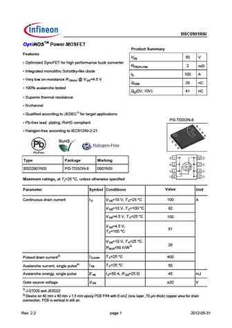
bsc0901ns bsc0901ns .pdf

n-Channel Power MOSFET OptiMOS BSC0901NS Data Sheet 2.1, 2011-09-23 Final Industrial & Multimarket OptiMOS Power-MOSFET BSC0901NS 1 Description OptiMOS 30V products are class leading power MOSFETs for highest power density and energy efficient solutions. Ultra low gate and output charges together with lowest on state resistance in small footprint packages make OptiMOS ... See More ⇒
9.9. Size:693K infineon
bsc0921ndi.pdf
BSC0921NDI Dual N-Channel OptiMOS MOSFET Product Summary Features Q1 Q2 Dual N-channel OptiMOS MOSFET VDS 30 30 V Optimized for high performance Buck converter RDS(on),max VGS=10 V 5 1.6 mW Logic level (4.5V rated) VGS=4.5 V 7 2.1 N-channel ID 40 40 A Qualified according to JEDEC1) for target applications Pb-free lead plating; RoHS compliant... See More ⇒
9.10. Size:1029K infineon
bsc0993nd.pdf
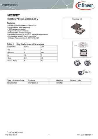
BSC0993ND MOSFET Powerstage 5x6 OptiMOSTM Power-MOSFET, 30 V Features Dual N-channel OptiMOS MOSFET Optimized for clean switching 100% avalanche tested Superior thermal resistance Optimized for wireless charger Qualified according to JEDEC1) for target applications Pb-free lead plating; RoHS compliant Halogen-free according to IEC61249-2-21 Table ... See More ⇒
9.11. Size:791K infineon
bsc0904nsi.pdf
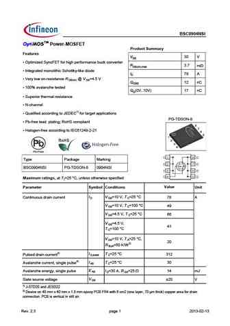
BSC0904NSI OptiMOSTM Power-MOSFET Product Summary Features VDS 30 V Optimized SyncFET for high performance buck converter RDS(on),max 3.7 mW Integrated monolithic Schottky-like diode ID 78 A Very low on-resistance R @ V =4.5 V DS(on) GS QOSS 12 nC 100% avalanche tested QG(0V..10V) 17 nC Superior thermal resistance N-channel Qualified accordin... See More ⇒
9.12. Size:1526K infineon
bsc0906ns.pdf

n-Channel Power MOSFET OptiMOS BSC0906NS Data Sheet 2.0, 2011-06-10 Final Industrial & Multimarket OptiMOS Power-MOSFET BSC0906NS 1 Description OptiMOS 30V products are class leading power MOSFETs for highest power density and energy efficient solutions. Ultra low gate and output charges together with lowest on state resistance in small footprint packages make OptiMOS ... See More ⇒
9.13. Size:1469K infineon
bsc0996ns.pdf
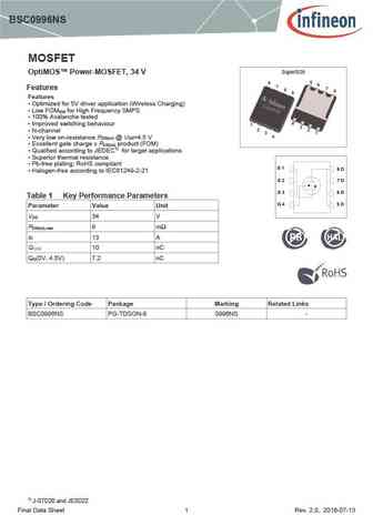
BSC0996NS MOSFET SuperSO8 OptiMOS Power-MOSFET, 34 V 5 8 6 7 Features 7 6 8 5 Features Optimized for 5V driver application (Wireless Charging) Low FOM for High Frequency SMPS SW 100% Avalanche tested 4 Improved switching behaviour 1 3 2 2 N-channel 3 1 4 Very low on-resistance R @ V =4.5 V DS(on) GS Excellent gate charge x R product (FOM)... See More ⇒
9.14. Size:686K infineon
bsc090n03ls.pdf
& " & E $;B1= !#& ' $=;0@/? &@99-=D Features D Q 2CD CG D49 ?8 ') - . 7@B -'*- m D n) m x 4 Q ) AD > J65 D649?@=@8I 7@B 4@?F6BD6BC D 1) Q + E2= 7 65 244@B5 ?8 D@ $ 7@B D2B86D 2AA= 42D @?C G D ON Q ( 492??6= &@8 4 =6F6= Q H46==6?D 82D6 492B86 H AB@5E4D ) ' D n) Q /6BI =@G @? B6C CD2?46 D n) Q -EA6B @B D96B>2= B6C CD2?46 Q F2=2?496 B2D65 Q *3 7B66 A=2D ?8 , @"... See More ⇒
9.15. Size:680K infineon
bsc090n03msg.pdf
% ! % D %0 S 07DK >AI A@ D7E;EF3@57 0 D n) G S J57>>7@F 93F7 5 3D97 J BDA6G5F !* ( D n) 1) S , G3>;8;76 355AD6;@9 FA % 8AD F3D97F 3BB>;53F;A@E S .GB7D;AD F 7D... See More ⇒
9.16. Size:658K infineon
bsc0902nsi.pdf
BSC0902NSI OptiMOSTM Power-MOSFET Product Summary Features VDS 30 V Optimized SyncFET for high performance buck converter RDS(on),max 2.8 mW Integrated monolithic Schottky-like diode ID 100 A Very low on-resistance R @ V =4.5 V DS(on) GS QOSS 17 nC 100% avalanche tested QG(0V..10V) 24 nC Superior thermal resistance N-channel Qualified accordi... See More ⇒
9.17. Size:1630K infineon
bsc0908ns rev3.2.pdf
n-Channel Power MOSFET OptiMOS BSC0908NS Data Sheet 3.2, 2011-09-26 Final Industrial & Multimarket OptiMOS Power-MOSFET BSC0908NS 1 Description OptiMOS 30V products are class leading power MOSFETs for highest power density and energy efficient solutions. Ultra low gate- and output charges together with lowest on state resistance in small footprint packages make OptiMOS ... See More ⇒
9.18. Size:679K infineon
bsc0911nd.pdf
BSC0911ND Dual N-Channel OptiMOS MOSFET Product Summary Features Q1 Q2 Dual N-channel OptiMOS MOSFET VDS 25 25 V Optimized for high performance Buck converter RDS(on),max VGS=10 V 3.2 1.2 mW Logic level (4.5V rated) VGS=4.5 V 4.8 1.7 N-channel ID 40 40 A Qualified according to JEDEC1) for target applications Pb-free lead plating; RoHS complia... See More ⇒
9.19. Size:580K infineon
bsc0901nsi.pdf
BSC0901NSI OptiMOSTM Power-MOSFET Product Summary Features VDS 30 V Optimized SyncFET for high performance buck converter RDS(on),max 2 mW Integrated monolithic Schottky-like diode ID 100 A Very low on-resistance R @ V =4.5 V DS(on) GS QOSS 28 nC 100% avalanche tested QG(0V..10V) 41 nC Superior thermal resistance N-channel Qualified according to JEDE... See More ⇒
9.20. Size:685K infineon
bsc0924ndi.pdf
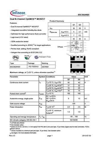
BSC0924NDI Dual N-Channel OptiMOS MOSFET Product Summary Features Q1 Q2 Dual N-channel OptiMOS MOSFET VDS 30 30 V Integrated monolithic Schottky-like diode RDS(on),max VGS=10 V 5 3.7 mW Optimized for high performance Buck converter VGS=4.5 V 7 5.2 Logic level (4.5V rated) ID 40 40 A 100% avalanche tested Qualified according to JEDEC1) for tar... See More ⇒
9.21. Size:608K infineon
bsc0909ns.pdf
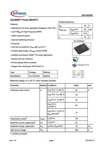
BSC0909NS OptiMOS Power-MOSFET Product Summary Features VDS 34 V Optimized for 5V driver application (Notebook, VGA, POL) RDS(on),max VGS=10 V 9.2 mW Low FOMSW for High Frequency SMPS VGS=4.5 V 11.8 100% Avalanche tested ID 44 A Improved switching behaviour PG-TDSON-8 N-channel Very low on-resistance R @ V =4.5 V DS(on) GS Excellent gate c... See More ⇒
9.23. Size:1052K infineon
bsc093n15ns5.pdf
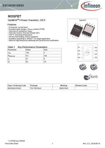
BSC093N15NS5 MOSFET SuperSO8 OptiMOSTM 5 Power-Transistor, 150 V 5 8 6 7 Features 7 6 8 5 N-channel, normal level Excellent gate charge x R product (FOM) DS(on) Very low on-resistance R DS(on) Very low reverse recovery charge (Qrr) 4 150 C operating temperature 1 3 2 2 Pb-free lead plating; RoHS compliant 3 1 4 Qualified according to JEDEC... See More ⇒
9.24. Size:684K infineon
bsc0910ndi.pdf
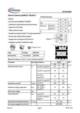
BSC0910NDI Dual N-Channel OptiMOS MOSFET Product Summary Features Q1 Q2 Dual N-channel OptiMOS MOSFET VDS 25 25 V Optimized for high performance Buck converter RDS(on),max VGS=10 V 4.6 1.2 mW Logic level (4.5V rated) VGS=4.5 V 5.9 1.6 100% avalanche tested ID 40 40 A Qualified according to JEDEC1) for target applications Pb-free lead plating;... See More ⇒
9.25. Size:1638K infineon
bsc0909ns rev3.2.pdf

n-Channel Power MOSFET OptiMOS BSC0909NS Data Sheet 3.2, 2011-09-26 Final Industrial & Multimarket OptiMOS Power-MOSFET BSC0909NS 1 Description OptiMOS 30V products are class leading power MOSFETs for highest power density and energy efficient solutions. Ultra low gate- and output charges together with lowest on state resistance in small footprint packages make OptiMOS ... See More ⇒
9.26. Size:1301K infineon
bsc097n06nst.pdf
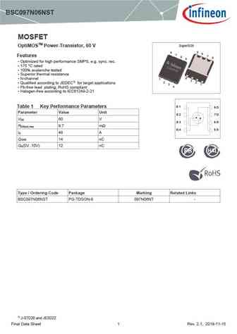
BSC097N06NST MOSFET SuperSO8 OptiMOSTM Power-Transistor, 60 V 5 8 6 7 Features 7 6 8 5 Optimized for high performance SMPS, e.g. sync. rec. 175 C rated 100% avalanche tested Superior thermal resistance 4 N-channel 1 3 2 2 Qualified according to JEDEC1) for target applications 3 1 4 Pb-free lead plating; RoHS compliant Halogen-free accor... See More ⇒
9.27. Size:483K infineon
bsc097n06ns.pdf
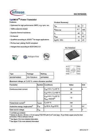
Type BSC097N06NS OptiMOSTM Power-Transistor Features Product Summary Optimized for high performance SMPS, e.g. sync. rec. VDS V 60 100% avalanche tested 9.7 RDS(on),max mW Superior thermal resistance ID A 46 N-channel QOSS nC 14 Qualified according to JEDEC1) for target applications QG(0V..10V) nC 12 Pb-free lead plating; RoHS complian... See More ⇒
Detailed specifications: BSC070N10NS5SC, BSC072N04LD, BSC074N15NS5, BSC076N04ND, BSC0804LS, BSC0805LS, BSC093N15NS5, BSC094N06LS5, 60N06, BSC097N06NST, BSC0993ND, BSC0996NS, BSC110N15NS5, BSC112N06LD, BSC13DN30NSFD, BSC146N10LS5, BSC155N06ND
Keywords - BSC096N10LS5 MOSFET specs
BSC096N10LS5 cross reference
BSC096N10LS5 equivalent finder
BSC096N10LS5 pdf lookup
BSC096N10LS5 substitution
BSC096N10LS5 replacement
Learn how to find the right MOSFET substitute. A guide to cross-reference, check specs and replace MOSFETs in your circuits.