ME20N03-G Specs and Replacement
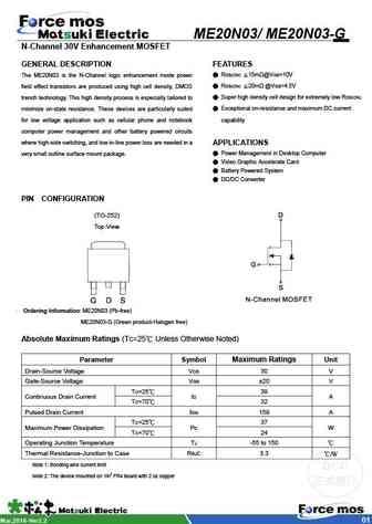
Type Designator: ME20N03-G
Type of Transistor: MOSFET
Type of Control Channel: N-Channel
Absolute Maximum Ratings
Pd ⓘ - Maximum Power Dissipation: 37 W
|Vds|ⓘ - Maximum Drain-Source Voltage: 30 V
|Vgs|ⓘ - Maximum Gate-Source Voltage: 20 V
|Id| ⓘ - Maximum Drain Current: 39 A
Tj ⓘ - Maximum Junction Temperature: 150 °C
Electrical Characteristics
tr ⓘ - Rise Time: 178 nS
Cossⓘ - Output Capacitance: 120 pF
RDSonⓘ - Maximum Drain-Source On-State Resistance: 0.015 Ohm
Package: TO252
ME20N03-G substitution
- MOSFET ⓘ Cross-Reference Search
ME20N03-G datasheet
me20n03 me20n03-g.pdf
ME20N03/ ME20N03-G N-Channel 30V Enhancement MOSFET GENERAL DESCRIPTION FEATURES The ME20N03 is the N-Channel logic enhancement mode power RDS(ON) 15m @VGS=10V field effect transistors are produced using high cell density, DMOS RDS(ON) 20m @VGS=4.5V trench technology. This high density process is especially tailored to Super high density cell design for extremel... See More ⇒
me20n03.pdf
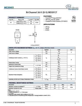
ME20N03 www.VBsemi.tw N-Channel 30-V (D-S) MOSFET FEATURES PRODUCT SUMMARY TrenchFET Power MOSFET VDS (V) RDS(on) ( ) ID (A)a, e Qg (Typ) 100 % Rg and UIS Tested Compliant to RoHS Directive 2011/65/EU 0.007 at VGS = 10 V 50 30 25 nC 0.009 at VGS = 4.5 V 40 APPLICATIONS D OR-ing Server TO-252 DC/DC G G D S S Top View N-Channel MOSFET ABSOLU... See More ⇒
me20n15 me20n15-g.pdf
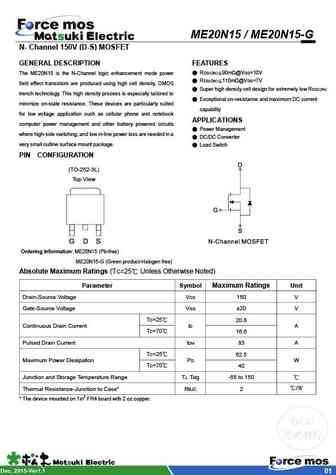
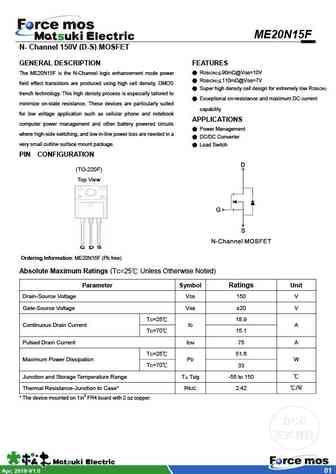
ME20N15 / ME20N15-G N- Channel 150V (D-S) MOSFET GENERAL DESCRIPTION FEATURES RDS(ON) 90m @VGS=10V The ME20N15 is the N-Channel logic enhancement mode power RDS(ON) 110m @VGS=7V field effect transistors are produced using high cell density, DMOS Super high density cell design for extremely low RDS(ON) trench technology. This high density process is especially t... See More ⇒
me20n10 me20n10-g.pdf
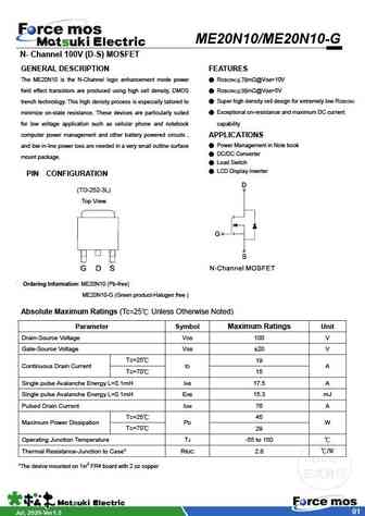
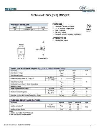
ME20N10/ME20N10-G N- Channel 100V (D-S) MOSFET GENERAL DESCRIPTION FEATURES The ME20N10 is the N-Channel logic enhancement mode power RDS(ON) 78m @VGS=10V field effect transistors are produced using high cell density, DMOS RDS(ON) 98m @VGS=5V trench technology. This high density process is especially tailored to Super high density cell design for extremely low RDS(ON)... See More ⇒
Detailed specifications: ME12N04, ME12N04-G, ME12N15, ME12N15-G, ME12P04, ME12P04-G, ME15N10-G, ME20N03, IRF520, ME20N15, ME20N15-G, ME20P03, ME20P03-G, ME20P06, ME20P06-G, ME2301, ME2301-G
Keywords - ME20N03-G MOSFET specs
ME20N03-G cross reference
ME20N03-G equivalent finder
ME20N03-G pdf lookup
ME20N03-G substitution
ME20N03-G replacement
Can't find your MOSFET? Learn how to find a substitute transistor by analyzing voltage, current and package compatibility
🌐 : EN ES РУ
LIST
Last Update
MOSFET: ASU70R600E | ASU65R850E | ASU65R550E | ASU65R350E | ASR65R120EFD | ASR65R046EFD | ASQ65R046EFD | ASM65R280E | ASM60R330E | ASE70R950E
Popular searches
a1941 | 2sd424 datasheet | 2sc536 datasheet | bd140 transistor equivalent | tip122 transistor equivalent | irfz44n equivalent | 2n2923 | 2n2102
