SI2324A Specs and Replacement
Type Designator: SI2324A
Type of Transistor: MOSFET
Type of Control Channel: N-Channel
Absolute Maximum Ratings
Pd ⓘ
- Maximum Power Dissipation: 1.2 W
|Vds|ⓘ - Maximum Drain-Source Voltage: 100 V
|Vgs|ⓘ - Maximum Gate-Source Voltage: 20 V
|Id| ⓘ - Maximum Drain Current: 2 A
Tj ⓘ - Maximum Junction Temperature: 150 °C
Electrical Characteristics
tr ⓘ - Rise Time: 52 nS
Cossⓘ -
Output Capacitance: 130 pF
RDSonⓘ - Maximum Drain-Source On-State Resistance: 0.28 Ohm
Package: SOT23
- MOSFET ⓘ Cross-Reference Search
SI2324A datasheet
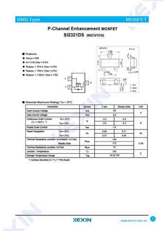
..1. Size:904K mcc
si2324a.pdf 
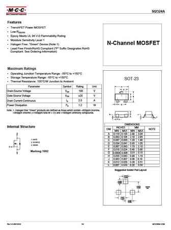
SI2324A Features TrenchFET Power MOSFET Low RDS(ON) Epoxy Meets UL 94 V-0 Flammability Rating Moisture Sensitivity Level 1 N-Channel MOSFET Halogen Free. Green Device (Note 1) Lead Free Finish/RoHS Compliant ("P" Suffix Designates RoHS Compliant. See Ordering Information) Maximum Ratings Operating Junction Temperature Range -55 C to +150 C S... See More ⇒
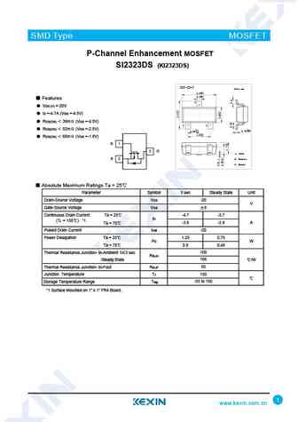
8.1. Size:2275K kexin
si2324ds.pdf
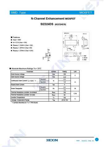
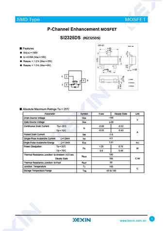
SMD Type MOSFET IC SMD Type N-Channel Enhancement MOSFET SI2324DS (KI2324DS) SOT-23-3 Unit mm +0.2 2.9-0.1 +0.1 0.4 -0.1 Features 3 VDSS = 100V ID = 2.3 A (VGS = 10V) RDS(ON) 234m (VGS = 10V) 1 2 +0.02 RDS(ON) 267m (VGS = 6V) +0.1 0.15 -0.02 0.95 -0.1 +0.1 1.9-0.2 D RDS(ON) 278m (VGS = 4.5V) 1. Gate 2. Source G 3. Drain... See More ⇒
8.2. Size:899K cn vbsemi
si2324ds-t1-ge3.pdf
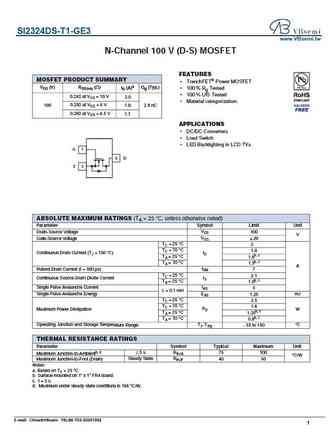
SI2324DS-T1-GE3 www.VBsemi.tw N-Channel 100 V (D-S) MOSFET FEATURES MOSFET PRODUCT SUMMARY TrenchFET Power MOSFET VDS (V) RDS(on) ( ) ID (A)a Qg (Typ.) 100 % Rg Tested 100 % UIS Tested 0.240 at VGS = 10 V 2.0 Material categorization 0.250 at VGS = 6 V 100 1.8 2.9 nC 0.260 at VGS = 4.5 V 1.7 APPLICATIONS DC/DC Converters Load Switch LED Back... See More ⇒
9.1. Size:188K vishay
si2325ds.pdf
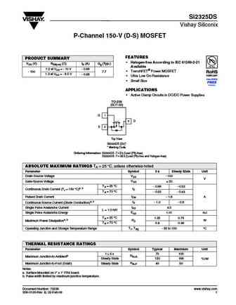
Si2325DS Vishay Siliconix P-Channel 150-V (D-S) MOSFET FEATURES PRODUCT SUMMARY Halogen-free According to IEC 61249-2-21 VDS (V) RDS(on) ( )ID (A) Qg (Typ.) Available 1.2 at VGS = - 10 V - 0.69 TrenchFET Power MOSFET - 150 7.7 1.3 at VGS = - 6.0 V - 0.66 Ultra Low On-Resistance Small Size APPLICATIONS Active Clamp Circuits in DC/DC Power Supplies T... See More ⇒
9.2. Size:205K vishay
si2321ds.pdf
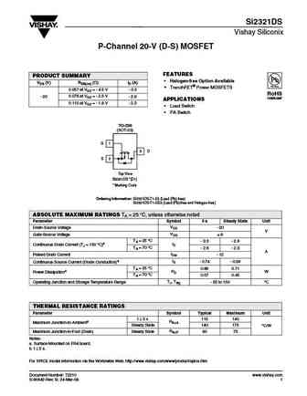
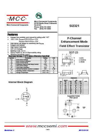
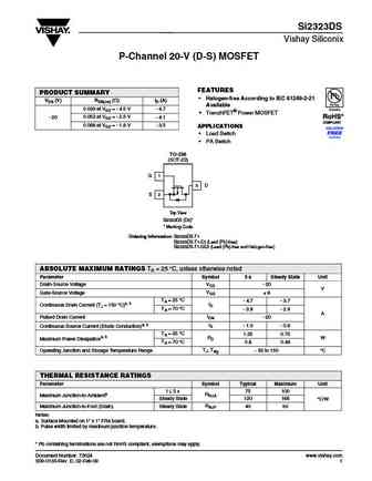
Si2321DS Vishay Siliconix P-Channel 20-V (D-S) MOSFET FEATURES PRODUCT SUMMARY Halogen-free Option Available VDS (V) RDS(on) ( )ID (A) TrenchFET Power MOSFETS 0.057 at VGS = - 4.5 V - 3.3 RoHS 0.076 at VGS = - 2.5 V - 20 - 2.8 COMPLIANT APPLICATIONS 0.110 at VGS = - 1.8 V - 2.3 Load Switch PA Switch TO-236 (SOT-23) G 1 3 D S 2 Top View Si2321... See More ⇒
9.3. Size:211K vishay
si2323dds.pdf
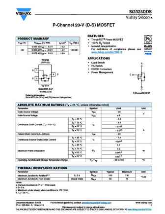
Si2323DDS Vishay Siliconix P-Channel 20-V (D-S) MOSFET FEATURES PRODUCT SUMMARY TrenchFET Power MOSFET VDS (V) RDS(on) ( ) Max. ID (A)d Qg (Typ.) 100 % Rg Tested Material categorization 0.039 at VGS = - 4.5 V - 5.3 For definitions of compliance please see - 20 0.050 at VGS = - 2.5 V - 4.7 13.6 nC www.vishay.com/doc?99912 0.075 at VGS = - 1.8 V - 3.8 APPLICATION... See More ⇒
9.5. Size:94K vishay
si2323cd si2323cds.pdf
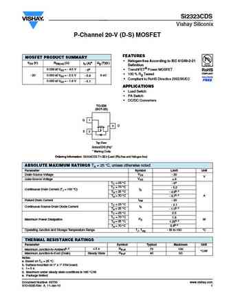
Si2323CDS Vishay Siliconix P-Channel 20-V (D-S) MOSFET FEATURES MOSFET PRODUCT SUMMARY Halogen-free According to IEC 61249-2-21 VDS (V) RDS(on) ( ) ID (A)a Qg (Typ.) Definition 0.039 at VGS = - 4.5 V TrenchFET Power MOSFET - 6e 100 % Rg Tested - 20 0.050 at VGS = - 2.5 V - 5.8 9 nC Compliant to RoHS Directive 2002/95/EC 0.063 at VGS = - 1.8 V - 5.1 APPLI... See More ⇒
9.6. Size:184K vishay
si2328ds.pdf
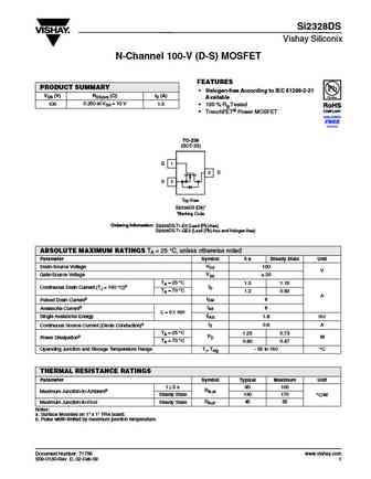
Si2328DS Vishay Siliconix N-Channel 100-V (D-S) MOSFET FEATURES PRODUCT SUMMARY Halogen-free According to IEC 61249-2-21 VDS (V) RDS(on) ( )ID (A) Available 0.250 at VGS = 10 V 100 1.5 100 % Rg Tested TrenchFET Power MOSFET TO-236 (SOT-23) G 1 3 D S 2 Top View Si2328DS (D8)* *Marking Code Ordering Information Si2328DS-T1-E3 (Lead (Pb)-free) Si2328DS-... See More ⇒
9.7. Size:191K vishay
si2327ds.pdf

Si2327DS Vishay Siliconix P-Channel 200-V (D-S) MOSFET FEATURES PRODUCT SUMMARY Halogen-free According to IEC 61249-2-21 VDS (V) RDS(on) ( )ID (A) Qg (Typ.) Available 2.35 at VGS = - 10 V - 0.49 TrenchFET Power MOSFET - 200 8.0 2.45 at VGS = - 6.0 V - 0.48 Ultra Low On-Resistance Small Size APPLICATIONS Active Clamp Circuits in DC/DC Power Supplies ... See More ⇒
9.8. Size:71K vishay
si2320ds.pdf
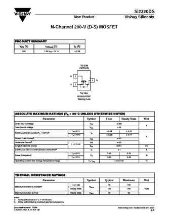
Si2320DS New Product Vishay Siliconix N-Channel 200-V (D-S) MOSFET PRODUCT SUMMARY VDS (V) rDS(on) (W) ID (A) 200 7 @ VGS = 10 V "0.28 TO-236 (SOT-23) G 1 3 D S 2 Top View Si2320DS (D0)* *Marking Code ABSOLUTE MAXIMUM RATINGS (TA = 25_C UNLESS OTHERWISE NOTED) Parameter Symbol 5 sec Steady State Unit Drain-Source Voltage VDS "200 V V Gate-Source Voltage VGS "20 TA= 25_C "0.... See More ⇒
9.9. Size:188K vishay
si2323ds.pdf
Si2323DS Vishay Siliconix P-Channel 20-V (D-S) MOSFET FEATURES PRODUCT SUMMARY Halogen-free According to IEC 61249-2-21 VDS (V) RDS(on) ( )ID (A) Available 0.039 at VGS = - 4.5 V - 4.7 TrenchFET Power MOSFET 0.052 at VGS = - 2.5 V - 20 - 4.1 0.068 at VGS = - 1.8 V - 3.5 APPLICATIONS Load Switch PA Switch TO-236 (SOT-23) G 1 3 D S 2 Top View S... See More ⇒
9.10. Size:223K vishay
si2329ds.pdf
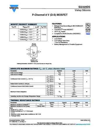
Si2329DS Vishay Siliconix P-Channel 8 V (D-S) MOSFET FEATURES MOSFET PRODUCT SUMMARY Halogen-free According to IEC 61249-2-21 VDS (V) RDS(on) ( ) ID (A)a Qg (Typ.) Definition 0.030 at VGS = - 4.5 V TrenchFET Power MOSFET - 6e 100 % Rg Tested 0.036 at VGS = - 2.5 V - 6e Compliant to RoHS Directive 2002/95/EC - 8 0.048 at VGS = - 1.8 V - 5.9 11.8 nC AP... See More ⇒
9.11. Size:217K vishay
si2323cds.pdf
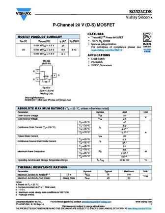
Si2323CDS Vishay Siliconix P-Channel 20 V (D-S) MOSFET FEATURES MOSFET PRODUCT SUMMARY TrenchFET Power MOSFET VDS (V) RDS(on) ( ) 100 % Rg Tested ID (A)a Qg (Typ.) Material categorization 0.039 at VGS = -4.5 V -6e For definitions of compliance please see -20 0.050 at VGS = -2.5 V -5.8 9 nC www.vishay.com/doc?99912 0.063 at VGS = -1.8 V -5.1 APPLICATIONS ... See More ⇒
9.12. Size:454K shenzhen
si2323.pdf
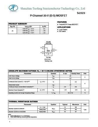
Shenzhen Tuofeng Semiconductor Technology Co., Ltd Si2323 P-Channel 20-V (D-S) MOSFET FEATURES PRODUCT SUMMARY D TrenchFETr Power MOSFET VDS (V) rDS(on) (W) ID (A) APPLICATIONS 0.043 @ VGS = -4.5 V -4.0 D Load Switch -20 0.054 @ VGS = -2.5 V - 4.0 D PA Switch 0.075 @ VGS = -1.8 V - 2.0 TO-236 (SOT-23) G 1 3 D S 2 Top View Si2323 (D3)* *Marking Code ABSOLUTE MAXIMUM RATINGS... See More ⇒
9.13. Size:298K shenzhen
si2328.pdf
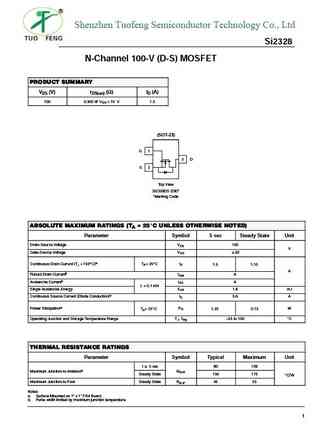
Shenzhen Tuofeng Semiconductor Technology Co., Ltd Si2328 N-Channel 100-V (D-S) MOSFET PRODUCT SUMMARY VDS (V) rDS(on) (W) ID (A) 100 0.300 @ VGS = 10 V 1.5 (SOT-23) G 1 3 D S 2 Top View Si2328DS (D8)* *Marking Code ABSOLUTE MAXIMUM RATINGS (TA = 25_C UNLESS OTHERWISE NOTED) Parameter Symbol 5 sec Steady State Unit Drain-Source Voltage VDS 100 V Gate-Source Voltage VGS "20 Con... See More ⇒
9.14. Size:1891K kexin
si2325ds.pdf
SMD Type MOSFET P-Channel Enhancement MOSFET SI2325DS (KI2325DS) SOT-23 Unit mm +0.1 2.9-0.1 Features +0.1 0.4 -0.1 VDS (V) =-150V 3 ID =-0.69A (VGS =-10V) RDS(ON) 1.2 (VGS =-10V) RDS(ON) 1.3 (VGS =-6V) 1 2 +0.05 0.95+0.1 -0.1 0.1 -0.01 1.9+0.1 -0.1 G 1 1.Gate 3 D 2.Source S 2 3.Drain Absolute Maximum Ratings Ta = 25 Param... See More ⇒
9.15. Size:1710K kexin
si2321ds.pdf
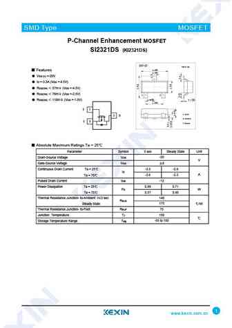
SMD Type MOSFET P-Channel Enhancement MOSFET SI2321DS (KI2321DS) SOT-23 Unit mm +0.1 2.9 -0.1 Features +0.1 0.4-0.1 VDS (V) =-20V 3 ID =-3.3A (VGS =-4.5V) RDS(ON) 57m (VGS =-4.5V) RDS(ON) 76m (VGS =-2.5V) 1 2 +0.1 +0.05 0.95 -0.1 0.1 -0.01 RDS(ON) 110m (VGS =-1.8V) +0.1 1.9 -0.1 G 1 1.Gate 3 D 2.Source S 2 3.Drain ... See More ⇒
9.16. Size:1626K kexin
si2328ds.pdf
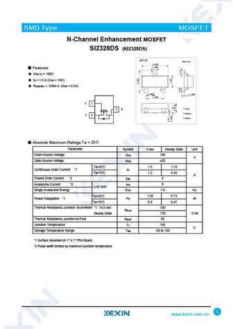
SMD Type MOSFET N-Channel Enhancement MOSFET SI2328DS (KI2328DS) SOT-23 Unit mm +0.1 2.9 -0.1 +0.1 0.4 -0.1 Features 3 VDS (V) = 100V ID = 1.5 A (VGS = 10V) RDS(ON) 250m (VGS = 4.5V) 1 2 +0.1 +0.05 0.95-0.1 0.1-0.01 +0.1 1.9-0.1 G 1 1.Gate 3 D 2.Source S 2 3.Drain Absolute Maximum Ratings Ta = 25 Parameter Symbol 5 sec Steady State Un... See More ⇒
9.17. Size:1691K kexin
si2323ds.pdf
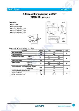
SMD Type MOSFET P-Channel Enhancement MOSFET SI2323DS (KI2323DS) SOT-23 Unit mm Features 2.9+0.1 -0.1 +0.1 0.4 -0.1 VDS (V) =-20V 3 ID =-4.7A (VGS =-4.5V) RDS(ON) 39m (VGS =-4.5V) RDS(ON) 52m (VGS =-2.5V) 1 2 RDS(ON) 68m (VGS =-1.8V) +0.1 +0.05 0.95 -0.1 0.1 -0.01 +0.1 1.9 -0.1 G 1 1.Gate 3 D 2.Source S 2 3.Drain A... See More ⇒
9.18. Size:1781K kexin
si2321ds-3.pdf
SMD Type MOSFET P-Channel Enhancement MOSFET SI2321DS (KI2321DS) SOT-23-3 Unit mm +0.2 2.9 -0.1 +0.1 0.4-0.1 Features 3 VDS (V) =-20V ID =-3.3A (VGS =-4.5V) RDS(ON) 57m (VGS =-4.5V) 1 2 RDS(ON) 76m (VGS =-2.5V) +0.02 +0.1 0.15 -0.02 0.95 -0.1 +0.1 1.9 -0.2 RDS(ON) 110m (VGS =-1.8V) G 1 3 D 1. Gate S 2 2. Source 3. Drai... See More ⇒
9.19. Size:1762K kexin
si2323ds-3.pdf
SMD Type MOSFET P-Channel Enhancement MOSFET SI2323DS (KI2323DS) SOT-23-3 Unit mm +0.2 2.9 -0.1 +0.1 0.4-0.1 Features 3 VDS (V) =-20V ID =-4.7A (VGS =-4.5V) RDS(ON) 39m (VGS =-4.5V) 1 2 RDS(ON) 52m (VGS =-2.5V) +0.02 +0.1 0.15 -0.02 0.95 -0.1 +0.1 1.9 -0.2 RDS(ON) 68m (VGS =-1.8V) G 1 3 D 1. Gate S 2 2. Source 3. Drain ... See More ⇒
9.21. Size:1953K kexin
si2325ds-3.pdf

SMD Type MOSFET P-Channel Enhancement MOSFET SI2325DS (KI2325DS) SOT-23-3 Unit mm +0.2 2.9 -0.1 +0.1 0.4 -0.1 Features 3 VDS (V) =-150V ID =-0.69A (VGS =-10V) RDS(ON) 1.2 (VGS =-10V) 1 2 +0.02 RDS(ON) 1.3 (VGS =-6V) +0.1 0.15 -0.02 0.95-0.1 +0.1 1.9-0.2 G 1 3 D 1. Gate S 2 2. Source 3. Drain Absolute Maximum Ratings Ta = 25 ... See More ⇒
9.22. Size:1853K umw-ic
si2328a.pdf
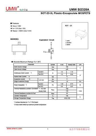
R UMW UMW SI2328A SOT-23-3L Plastic-Encapsulate MOSFETS Features SOT 23 VDS (V) = 100V ID = 1.5 A (VGS = 10V) RDS(ON) 250m (VGS = 4.5V) MARKING Equivalent Circuit 1. GATE 2. SOURCE D 3. DRAIN G S Absolute Maximum Ratings Ta = 25 Parameter Symbol 5 sec Steady State Unit Drain-Source Voltage VDS 100 V Gate-Source Voltage VGS 20 Ta=... See More ⇒
9.23. Size:1931K born
si2328.pdf
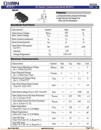
SI2328 MOSFET ROHS N-Channel Enhancement-Mode MOSFET SOT-23 - Features Advanced trench process technology High Density Cell Design For Ultra Low On-Resistance MAXIMUM RANTINGS Characteristic Symbol Max Unit 100 Drain-Source Voltage BV V DSS Gate- Source Voltage V V GS +20 Drain Current (continuous) I 1.5 A D Drain Current (pulsed) I A DM 6 Total Device Dissipa... See More ⇒
9.24. Size:866K cn vbsemi
si2323cds-t1-ge3.pdf

SI2323CDS-T1-GE3 www.VBsemi.tw P-Channel 30 V (D-S) MOSFET FEATURES PRODUCT SUMMARY TrenchFET Power MOSFET 100 % Rg Tested VDS (V) RDS(on) ( ) Typ. ID (A)a Qg (Typ.) 0.046 at VGS = - 10 V - 5.6 0.049 at VGS = - 6 V - 5 11.4 nC - 30 APPLICATIONS 0.054 at VGS = - 4.5 V -4.5 For Mobile Computing - Load Switch - Notebook Adaptor Switch S TO-236 - DC/DC Converter ... See More ⇒
9.25. Size:905K cn vbsemi
si2323ds-t1.pdf
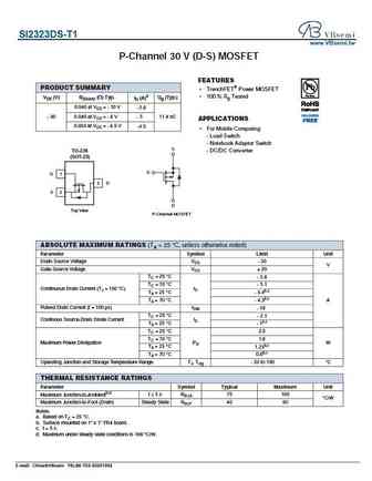
SI2323DS-T1 www.VBsemi.tw P-Channel 30 V (D-S) MOSFET FEATURES PRODUCT SUMMARY TrenchFET Power MOSFET 100 % Rg Tested VDS (V) RDS(on) ( ) Typ. ID (A)a Qg (Typ.) 0.046 at VGS = - 10 V - 5.6 0.049 at VGS = - 6 V - 5 11.4 nC - 30 APPLICATIONS 0.054 at VGS = - 4.5 V -4.5 For Mobile Computing - Load Switch - Notebook Adaptor Switch S TO-236 - DC/DC Converter (SOT... See More ⇒
9.26. Size:1370K cn vbsemi
si2328ds.pdf
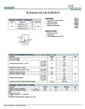
SI2328DS www.VBsemi.tw N-Channel 100 V (D-S) MOSFET FEATURES MOSFET PRODUCT SUMMARY TrenchFET Power MOSFET VDS (V) RDS(on) ( ) ID (A)a Qg (Typ.) 100 % Rg Tested 100 % UIS Tested 0.240 at VGS = 10 V 2.0 Material categorization 0.250 at VGS = 6 V 100 1.8 2.9 nC 0.260 at VGS = 4.5 V 1.7 APPLICATIONS DC/DC Converters Load Switch LED Backlightin... See More ⇒
9.27. Size:868K cn vbsemi
si2323dds-t1-ge3.pdf
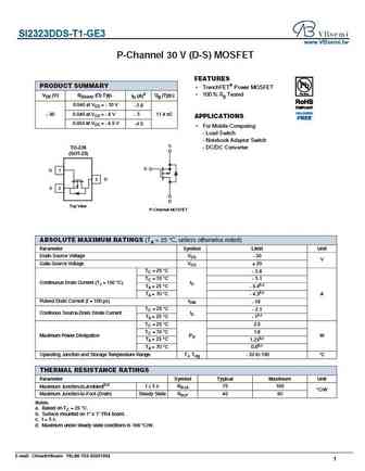
SI2323DDS-T1-GE3 www.VBsemi.tw P-Channel 30 V (D-S) MOSFET FEATURES PRODUCT SUMMARY TrenchFET Power MOSFET 100 % Rg Tested VDS (V) RDS(on) ( ) Typ. ID (A)a Qg (Typ.) 0.046 at VGS = - 10 V - 5.6 0.049 at VGS = - 6 V - 5 11.4 nC - 30 APPLICATIONS 0.054 at VGS = - 4.5 V -4.5 For Mobile Computing - Load Switch - Notebook Adaptor Switch S TO-236 - DC/DC Converter ... See More ⇒
Detailed specifications: MCU80N06A, MSJAC11N65Y, MSJU11N65, SI1012, SI2101, SI2310A, SI2310B, SI2312B, NCEP15T14, SI3134KDW, SI3134KL3, SI3139KE, SI3139KL3, SI3400A, SI3401A, SI3402, SI3407
Keywords - SI2324A MOSFET specs
SI2324A cross reference
SI2324A equivalent finder
SI2324A pdf lookup
SI2324A substitution
SI2324A replacement
Learn how to find the right MOSFET substitute. A guide to cross-reference, check specs and replace MOSFETs in your circuits.