PSMN2R0-25YLD Datasheet. Specs and Replacement
Type Designator: PSMN2R0-25YLD 📄📄
Type of Transistor: MOSFET
Type of Control Channel: N-Channel
Absolute Maximum Ratings
Pd ⓘ - Maximum Power Dissipation: 115 W
|Vds|ⓘ - Maximum Drain-Source Voltage: 25 V
|Vgs|ⓘ - Maximum Gate-Source Voltage: 20 V
|Id| ⓘ - Maximum Drain Current: 100 A
Tj ⓘ - Maximum Junction Temperature: 175 °C
Electrical Characteristics
tr ⓘ - Rise Time: 18.7 nS
Cossⓘ - Output Capacitance: 1142 pF
RDSonⓘ - Maximum Drain-Source On-State Resistance: 0.00209 Ohm
Package: SOT669
📄📄 Copy
PSMN2R0-25YLD substitution
- MOSFET ⓘ Cross-Reference Search
PSMN2R0-25YLD datasheet
..1. Size:724K nxp
psmn2r0-25yld.pdf 
PSMN2R0-25YLD N-channel 25 V, 2.09 m , 140 A logic level MOSFET in LFPAK56 using NextPowerS3 Technology 19 April 2016 Product data sheet 1. General description Logic level gate drive N-channel enhancement mode MOSFET in LFPAK56 package. NextPowerS3 portfolio utilising Nexperia s unique SchottkyPlus technology delivers high efficiency, low spiking performance usually associated w... See More ⇒
4.1. Size:728K nxp
psmn2r0-25mld.pdf
PSMN2R0-25MLD N-channel 25 V, 2.1 m logic level MOSFET in LFPAK33 using NextPowerS3 Technology 8 April 2016 Product data sheet 1. General description Logic level gate drive N-channel enhancement mode MOSFET in LFPAK33 package. NextPowerS3 portfolio utilising Nexperia s unique SchottkyPlus technology delivers high efficiency, low spiking performance usually associated with MOSFE... See More ⇒
6.1. Size:231K philips
psmn2r0-60es.pdf
PSMN2R0-60ES N-channel 60 V 2.2 m standard level MOSFET in I2PAK Rev. 02 19 April 2011 Product data sheet 1. Product profile 1.1 General description Standard level N-channel MOSFET in a I2PAK package qualified to 175 C. This product is designed and qualified for use in a wide range of industrial, communications and domestic equipment. 1.2 Features and benefits High efficien... See More ⇒
6.2. Size:238K philips
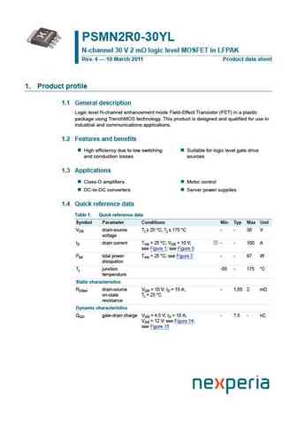
psmn2r0-30yl.pdf
PSMN2R0-30YL N-channel 30 V 2 m logic level MOSFET in LFPAK Rev. 4 10 March 2011 Product data sheet 1. Product profile 1.1 General description Logic level N-channel enhancement mode Field-Effect Transistor (FET) in a plastic package using TrenchMOS technology. This product is designed and qualified for use in industrial and communications applications. 1.2 Features and benefits... See More ⇒
6.3. Size:237K philips
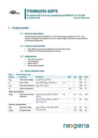
psmn2r0-60ps.pdf
PSMN2R0-60PS N-channel 60 V 2.2 m standard level MOSFET in TO-220 Rev. 02 19 April 2011 Product data sheet 1. Product profile 1.1 General description Standard level N-channel MOSFET in a TO-220 package qualified to 175 C. This product is designed and qualified for use in a wide range of industrial, communications and domestic equipment. 1.2 Features and benefits High effici... See More ⇒
6.4. Size:212K philips
psmn2r0-30pl.pdf
PSMN2R0-30PL N-channel 30 V 2.1 m logic level MOSFET Rev. 01 24 June 2009 Product data sheet 1. Product profile 1.1 General description Logic level N-channel MOSFET in TO220 package qualified to 175 C. This product is designed and qualified for use in a wide range of industrial, communications and domestic equipment. 1.2 Features and benefits High efficiency due to low swit... See More ⇒
6.5. Size:221K nxp
psmn2r0-30yle.pdf
PSMN2R0-30YLE N-channel 30 V 2 m logic level MOSFET in LFPAK 12 October 2012 Product data sheet 1. Product profile 1.1 General description Logic level N-channel MOSFET in LFPAK package qualified to 175 C. This product is designed and qualified for use in a wide range of industrial, communications and domestic equipment. 1.2 Features and benefits Enhanced forward biased safe op... See More ⇒
6.6. Size:820K nxp
psmn2r0-60es.pdf
PSMN2R0-60ES N-channel 60 V 2.2 m standard level MOSFET in I2PAK Rev. 02 19 April 2011 Product data sheet 1. Product profile 1.1 General description Standard level N-channel MOSFET in a I2PAK package qualified to 175 C. This product is designed and qualified for use in a wide range of industrial, communications and domestic equipment. 1.2 Features and benefits High efficien... See More ⇒
6.7. Size:823K nxp
psmn2r0-30yl.pdf
PSMN2R0-30YL N-channel 30 V 2 m logic level MOSFET in LFPAK Rev. 4 10 March 2011 Product data sheet 1. Product profile 1.1 General description Logic level N-channel enhancement mode Field-Effect Transistor (FET) in a plastic package using TrenchMOS technology. This product is designed and qualified for use in industrial and communications applications. 1.2 Features and benefits... See More ⇒
6.8. Size:380K nxp
psmn2r0-60psr.pdf
Important notice Dear Customer, On 7 February 2017 the former NXP Standard Product business became a new company with the tradename Nexperia. Nexperia is an industry leading supplier of Discrete, Logic and PowerMOS semiconductors with its focus on the automotive, industrial, computing, consumer and wearable application markets In data sheets and application notes which still contain... See More ⇒
6.9. Size:742K nxp
psmn2r0-60ps.pdf
PSMN2R0-60PS N-channel 60 V 2.2 m standard level MOSFET in TO-220 4 October 2012 Product data sheet 1. Product profile 1.1 General description Standard level N-channel MOSFET in a TO-220 package qualified to 175 C. This product is designed and qualified for use in a wide range of industrial, communications and domestic equipment. 1.2 Features and benefits High efficiency due to... See More ⇒
6.10. Size:230K nxp
psmn2r0-30yld.pdf
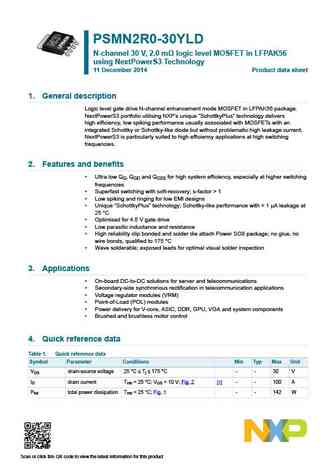
PSMN2R0-30YLD N-channel 30 V, 2.0 m logic level MOSFET in LFPAK56 using NextPowerS3 Technology 11 December 2014 Product data sheet 1. General description Logic level gate drive N-channel enhancement mode MOSFET in LFPAK56 package. NextPowerS3 portfolio utilising NXP s unique SchottkyPlus technology delivers high efficiency, low spiking performance usually associated with MOSFET... See More ⇒
6.11. Size:713K nxp
psmn2r0-30pl.pdf
PSMN2R0-30PL N-channel 30 V 2.1 m logic level MOSFET Rev. 01 24 June 2009 Product data sheet 1. Product profile 1.1 General description Logic level N-channel MOSFET in TO220 package qualified to 175 C. This product is designed and qualified for use in a wide range of industrial, communications and domestic equipment. 1.2 Features and benefits High efficiency due to low swit... See More ⇒
6.12. Size:302K nxp
psmn2r0-40yld.pdf
PSMN2R0-40YLD N-channel 40 V, 2.1 m , 180 A logic level MOSFET in LFPAK56 using NextPower-S3 Schottky-Plus technology 25 September 2019 Product data sheet 1. General description 180 A, logic level gate drive N-channel enhancement mode MOSFET in 175 C LFPAK56 package using advanced TrenchMOS Superjunction technology. This product has been designed and qualified for high performance pow... See More ⇒
6.13. Size:208K nxp
psmn2r0-30bl.pdf
PSMN2R0-30BL N-channel 30 V 2.1 m logic level MOSFET in D2PAK Rev. 1 20 March 2012 Product data sheet 1. Product profile 1.1 General description Logic level N-channel MOSFET in D2PAK package qualified to 175 C. This product is designed and qualified for use in a wide range of industrial, communications and domestic equipment. 1.2 Features and benefits High efficiency due... See More ⇒
6.14. Size:255K inchange semiconductor
psmn2r0-60es.pdf
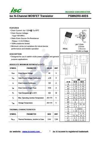
isc N-Channel MOSFET Transistor PSMN2R0-60ES FEATURES Drain Current I = 120A@ T =25 D C Drain Source Voltage- V = 60V(Min) DSS Static Drain-Source On-Resistance R = 2.2m (Max) DS(on) 100% avalanche tested Minimum Lot-to-Lot variations for robust device performance and reliable operation DESCRIPTION Designed for use in switch mode power supplies and general ... See More ⇒
6.15. Size:261K inchange semiconductor
psmn2r0-60ps.pdf
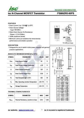
isc N-Channel MOSFET Transistor PSMN2R0-60PS FEATURES Drain Current I = 120A@ T =25 D C Drain Source Voltage- V = 60V(Min) DSS Static Drain-Source On-Resistance R = 2.2m (Max) DS(on) 100% avalanche tested Minimum Lot-to-Lot variations for robust device performance and reliable operation DESCRIPTION Designed for use in switch mode power supplies and general ... See More ⇒
6.16. Size:261K inchange semiconductor
psmn2r0-30pl.pdf
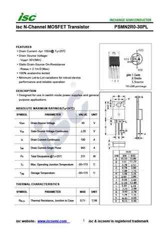
isc N-Channel MOSFET Transistor PSMN2R0-30PL FEATURES Drain Current I = 100A@ T =25 D C Drain Source Voltage- V = 30V(Min) DSS Static Drain-Source On-Resistance R = 2.1m (Max) DS(on) 100% avalanche tested Minimum Lot-to-Lot variations for robust device performance and reliable operation DESCRIPTION Designed for use in switch mode power supplies and general ... See More ⇒
6.17. Size:254K inchange semiconductor
psmn2r0-30bl.pdf
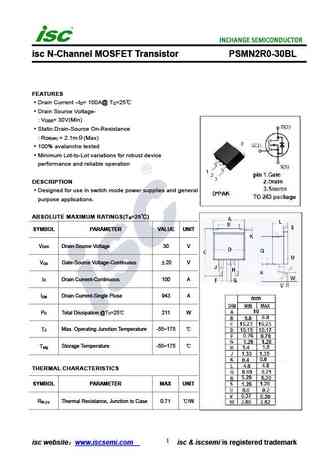
isc N-Channel MOSFET Transistor PSMN2R0-30BL FEATURES Drain Current I = 100A@ T =25 D C Drain Source Voltage- V = 30V(Min) DSS Static Drain-Source On-Resistance R = 2.1m (Max) DS(on) 100% avalanche tested Minimum Lot-to-Lot variations for robust device performance and reliable operation DESCRIPTION Designed for use in switch mode power supplies and general ... See More ⇒
Detailed specifications: PSMN1R5-25MLH, PSMN1R5-40YSD, PSMN1R6-30MLH, PSMN1R7-25YLD, PSMN1R7-40YLD, PSMN1R8-30MLH, PSMN1R9-40YSD, PSMN2R0-25MLD, IRF9640, PSMN2R0-40YLD, PSMN2R0-60PSR, PSMN2R2-40YSD, PSMN2R5-40YLD, PSMN2R8-40YSD, PSMN3R2-40YLD, PSMN3R3-40MLH, PSMN3R3-40MSH
Keywords - PSMN2R0-25YLD MOSFET specs
PSMN2R0-25YLD cross reference
PSMN2R0-25YLD equivalent finder
PSMN2R0-25YLD pdf lookup
PSMN2R0-25YLD substitution
PSMN2R0-25YLD replacement
Step-by-step guide to finding a MOSFET replacement. Cross-reference parts and ensure compatibility for your repair or project.
