NVMFS5C456N Specs and Replacement
Type Designator: NVMFS5C456N
Type of Transistor: MOSFET
Type of Control Channel: N-Channel
Absolute Maximum Ratings
Pd ⓘ - Maximum Power Dissipation: 55 W
|Vds|ⓘ - Maximum Drain-Source Voltage: 40 V
|Vgs|ⓘ - Maximum Gate-Source Voltage: 20 V
|Id| ⓘ - Maximum Drain Current: 80 A
Tj ⓘ - Maximum Junction Temperature: 175 °C
Electrical Characteristics
tr ⓘ - Rise Time: 80 nS
Cossⓘ - Output Capacitance: 600 pF
RDSonⓘ - Maximum Drain-Source On-State Resistance: 0.0045 Ohm
Package: DFN5
NVMFS5C456N substitution
- MOSFET ⓘ Cross-Reference Search
NVMFS5C456N datasheet
nvmfs5c456n.pdf
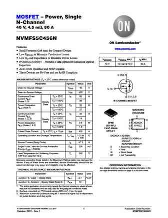
MOSFET Power, Single N-Channel 40 V, 4.5 mW, 80 A NVMFS5C456N Features www.onsemi.com Small Footprint (5x6 mm) for Compact Design Low RDS(on) to Minimize Conduction Losses Low QG and Capacitance to Minimize Driver Losses V(BR)DSS RDS(ON) MAX ID MAX NVMFS5C456NWF - Wettable Flank Option for Enhanced Optical 40 V 4.5 mW @ 10 V 80 A Inspection AEC-Q101 Qualifie... See More ⇒
nvmfs5c450nl.pdf
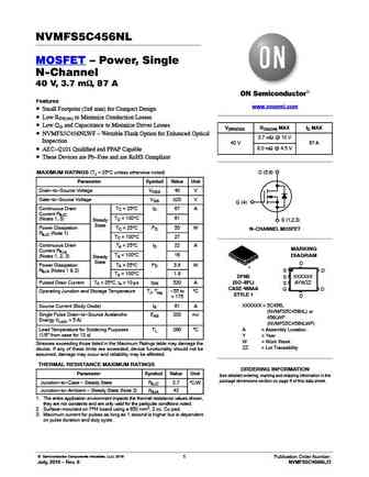
NVMFS5C450NL Power MOSFET 40 V, 2.8 mW, 110 A, Single N-Channel Features Small Footprint (5x6 mm) for Compact Design Low RDS(on) to Minimize Conduction Losses www.onsemi.com Low QG and Capacitance to Minimize Driver Losses NVMFS5C450NLWF - Wettable Flank Option for Enhanced Optical Inspection V(BR)DSS RDS(ON) MAX ID MAX AEC-Q101 Qualified and PPAP Capable 2.8 mW ... See More ⇒
nvmfs5c450n.pdf
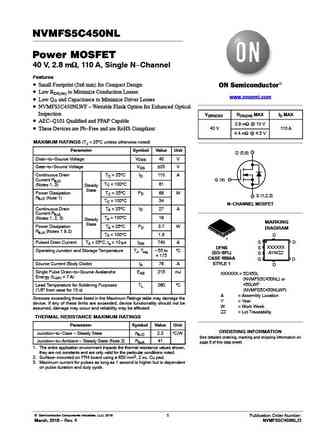
NVMFS5C450N MOSFET Power, Single N-Channel 40 V, 3.3 mW, 102 A Features www.onsemi.com Small Footprint (5x6 mm) for Compact Design Low RDS(on) to Minimize Conduction Losses Low QG and Capacitance to Minimize Driver Losses V(BR)DSS RDS(ON) MAX ID MAX NVMFS5C450NWF - Wettable Flank Option for Enhanced Optical 40 V 3.3 mW @ 10 V 102 A Inspection AEC-Q101 Qualif... See More ⇒
Detailed specifications: NVMFS5C410N, NVMFS5C426N, NVMFS5C426NL, NVMFS5C430N, NVMFS5C430NL, NVMFS5C442N, NVMFS5C450N, NVMFS5C450NL, IRLB4132, NVMFS5C456NL, NVMFS5C460N, NVMFS5C460NL, NVMFS5C466N, NVMFS5C468N, NVMFS5C468NL, NVMFS5C612N, NVMFS5C628N
Keywords - NVMFS5C456N MOSFET specs
NVMFS5C456N cross reference
NVMFS5C456N equivalent finder
NVMFS5C456N pdf lookup
NVMFS5C456N substitution
NVMFS5C456N replacement
Step-by-step guide to finding a MOSFET replacement. Cross-reference parts and ensure compatibility for your repair or project.
History: SQ2337ES
🌐 : EN ES РУ

LIST
Last Update
MOSFET: FTF30P35D | FTF25N35DHVT | FTF15N35D | FTE15C35G | FTP02P15G | FTE02P15G | AKF30N5P0SX | AKF30N10S | AKF20P45D | CM4407
Popular searches
2024ont | 2n1306 transistor | 2sa750 datasheet | 2sa940 transistor datasheet | 2sb549 | 5n50 mosfet equivalent | a1016 transistor | a1693 transistor