NVMFS6B75NL Specs and Replacement
Type Designator: NVMFS6B75NL
Type of Transistor: MOSFET
Type of Control Channel: N-Channel
Absolute Maximum Ratings
Pd ⓘ
- Maximum Power Dissipation: 56 W
|Vds|ⓘ - Maximum Drain-Source Voltage: 100 V
|Vgs|ⓘ - Maximum Gate-Source Voltage: 16 V
|Id| ⓘ - Maximum Drain Current: 28 A
Tj ⓘ - Maximum Junction Temperature: 175 °C
Electrical Characteristics
tr ⓘ - Rise Time: 88.3 nS
Cossⓘ -
Output Capacitance: 260 pF
Rds ⓘ - Maximum Drain-Source On-State Resistance: 0.03 Ohm
Package: DFN5
- MOSFET ⓘ Cross-Reference Search
NVMFS6B75NL datasheet
..1. Size:121K onsemi
nvmfs6b75nl.pdf 
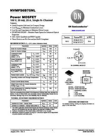
NVMFS6B75NL Power MOSFET 100 V, 30 mW, 28 A, Single N-Channel Features Small Footprint (5x6 mm) for Compact Design Low RDS(on) to Minimize Conduction Losses Low QG and Capacitance to Minimize Driver Losses www.onsemi.com NVMFS6B75NLWF - Wettable Flank Option for Enhanced Optical Inspection AEC-Q101 Qualified and PPAP Capable V(BR)DSS RDS(ON) MAX ID MAX These ... See More ⇒
7.1. Size:79K onsemi
nvmfs6b14nl.pdf
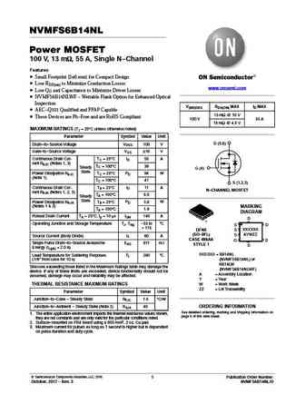
NVMFS6B14NL Power MOSFET 100 V, 13 mW, 55 A, Single N-Channel Features Small Footprint (5x6 mm) for Compact Design Low RDS(on) to Minimize Conduction Losses www.onsemi.com Low QG and Capacitance to Minimize Driver Losses NVMFS6B14NLWF - Wettable Flank Option for Enhanced Optical Inspection V(BR)DSS RDS(ON) MAX ID MAX AEC-Q101 Qualified and PPAP Capable 13 mW @ 10... See More ⇒
8.1. Size:174K onsemi
nvmfs6h858nl.pdf
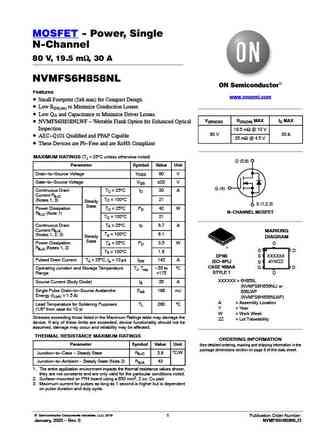
MOSFET - Power, Single N-Channel 80 V, 19.5 mW, 30 A NVMFS6H858NL Features www.onsemi.com Small Footprint (5x6 mm) for Compact Design Low RDS(on) to Minimize Conduction Losses Low QG and Capacitance to Minimize Driver Losses V(BR)DSS RDS(ON) MAX ID MAX NVMFS6H858NLWF - Wettable Flank Option for Enhanced Optical Inspection 19.5 mW @ 10 V 80 V 30 A AEC-Q101 Quali... See More ⇒
8.2. Size:176K onsemi
nvmfs6h824n.pdf

MOSFET - Power, Single N-Channel 80 V, 4.5 mW, 107 A NVMFS6H824N Features www.onsemi.com Small Footprint (5x6 mm) for Compact Design Low RDS(on) to Minimize Conduction Losses Low QG and Capacitance to Minimize Driver Losses NVMFS6H824NWF - Wettable Flank Option for Enhanced Optical V(BR)DSS RDS(ON) MAX ID MAX Inspection 80 V 4.5 mW @ 10 V 107 A AEC-Q101 Qualifie... See More ⇒
8.3. Size:174K onsemi
nvmfs6h818n.pdf
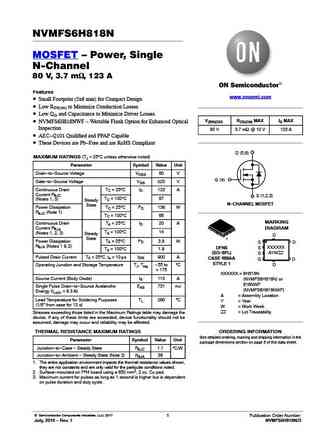
NVMFS6H818N MOSFET Power, Single N-Channel 80 V, 3.7 mW, 123 A Features www.onsemi.com Small Footprint (5x6 mm) for Compact Design Low RDS(on) to Minimize Conduction Losses Low QG and Capacitance to Minimize Driver Losses V(BR)DSS RDS(ON) MAX ID MAX NVMFS6H818NWF - Wettable Flank Option for Enhanced Optical Inspection 80 V 3.7 mW @ 10 V 123 A AEC-Q101 Qualif... See More ⇒
8.4. Size:177K onsemi
nvmfs6h848n.pdf

MOSFET - Power, Single N-Channel 80 V, 9.4 mW, 64 A NVMFS6H848N Features www.onsemi.com Small Footprint (5x6 mm) for Compact Design Low RDS(on) to Minimize Conduction Losses Low QG and Capacitance to Minimize Driver Losses NVMFS6H848NWF - Wettable Flank Option for Enhanced Optical V(BR)DSS RDS(ON) MAX ID MAX Inspection 80 V 9.4 mW @ 10 V 64 A AEC-Q101 Qualified ... See More ⇒
8.5. Size:172K onsemi
nvmfs6h801nl.pdf

MOSFET - Power, Single N-Channel 80 V, 2.7 mW, 160 A NVMFS6H801NL Features www.onsemi.com Small Footprint (5x6 mm) for Compact Design Low RDS(on) to Minimize Conduction Losses Low QG and Capacitance to Minimize Driver Losses NVMFS6H801NLWF - Wettable Flank Option for Enhanced Optical V(BR)DSS RDS(ON) MAX ID MAX Inspection 2.7 mW @ 10 V AEC-Q101 Qualified and PPA... See More ⇒
8.6. Size:178K onsemi
nvmfs6h852n.pdf
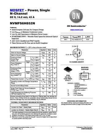
MOSFET - Power, Single N-Channel 80 V, 14.2 mW, 43 A NVMFS6H852N Features www.onsemi.com Small Footprint (5x6 mm) for Compact Design Low RDS(on) to Minimize Conduction Losses Low QG and Capacitance to Minimize Driver Losses NVMFS6H852NWF - Wettable Flank Option for Enhanced Optical V(BR)DSS RDS(ON) MAX ID MAX Inspection 80 V 14.2 mW @ 10 V 43 A AEC-Q101 Qualifie... See More ⇒
8.7. Size:180K onsemi
nvmfs6h864n.pdf
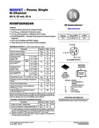
MOSFET - Power, Single N-Channel 80 V, 32 mW, 23 A NVMFS6H864N Features www.onsemi.com Small Footprint (5x6 mm) for Compact Design Low RDS(on) to Minimize Conduction Losses Low QG and Capacitance to Minimize Driver Losses V(BR)DSS RDS(ON) MAX ID MAX NVMFS6H864NWF - Wettable Flank Option for Enhanced Optical 80 V 32 mW @ 10 V 23 A Inspection AEC-Q101 Qualified an... See More ⇒
8.8. Size:134K onsemi
nvmfs6d1n08h.pdf
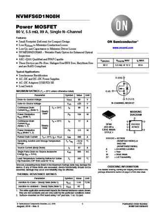
NVMFS6D1N08H Power MOSFET 80 V, 5.5 mW, 89 A, Single N-Channel Features Small Footprint (5x6 mm) for Compact Design Low RDS(on) to Minimize Conduction Losses www.onsemi.com Low QG and Capacitance to Minimize Driver Losses NVMFSW6D1N08H - Wettable Flank Option for Enhanced Optical Inspection AEC-Q101 Qualified and PPAP Capable V(BR)DSS RDS(ON) MAX ID MAX These... See More ⇒
8.9. Size:172K onsemi
nvmfs6h818nl.pdf
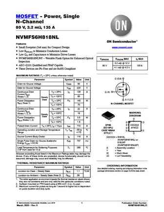
MOSFET - Power, Single N-Channel 80 V, 3.2 mW, 135 A NVMFS6H818NL Features www.onsemi.com Small Footprint (5x6 mm) for Compact Design Low RDS(on) to Minimize Conduction Losses Low QG and Capacitance to Minimize Driver Losses NVMFS6H818NLWF - Wettable Flank Option for Enhanced Optical V(BR)DSS RDS(ON) MAX ID MAX Inspection 3.2 mW @ 10 V AEC-Q101 Qualified and PPA... See More ⇒
8.10. Size:203K onsemi
nvmfs6h801n.pdf

MOSFET Power, Single, N-Channel 80 V, 2.8 mW, 157 A NVMFS6H801N Features www.onsemi.com Small Footprint (5x6 mm) for Compact Design Low RDS(on) to Minimize Conduction Losses Low QG and Capacitance to Minimize Driver Losses V(BR)DSS RDS(ON) MAX ID MAX NVMFS6H801NWF - Wettable Flank Option for Enhanced Optical Inspection 80 V 2.8 mW @ 10 V 157 A AEC-Q101 Quali... See More ⇒
8.11. Size:196K onsemi
nvmfs6h800nl.pdf
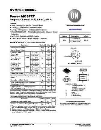
NVMFS6H800NL Power MOSFET Single N-Channel, 80 V, 1.9 mW, 224 A Features Small Footprint (5x6 mm) for Compact Design Low RDS(on) to Minimize Conduction Losses www.onsemi.com Low QG and Capacitance to Minimize Driver Losses NVMFS6H800NLWF - Wettable Flank Option for Enhanced Optical Inspection V(BR)DSS RDS(ON) MAX ID MAX AEC-Q101 Qualified and PPAP Capable The... See More ⇒
8.12. Size:175K onsemi
nvmfs6h836nl.pdf

MOSFET - Power, Single N-Channel 80 V, 6.2 mW, 77 A NVMFS6H836NL Features www.onsemi.com Small Footprint (5x6 mm) for Compact Design Low RDS(on) to Minimize Conduction Losses Low QG and Capacitance to Minimize Driver Losses V(BR)DSS RDS(ON) MAX ID MAX NVMFS6H836NLWF - Wettable Flank Option for Enhanced Optical Inspection 6.2 mW @ 10 V 80 V 77 A AEC-Q101 Qualif... See More ⇒
8.13. Size:176K onsemi
nvmfs6h836n.pdf

MOSFET - Power, Single N-Channel 80 V, 6.7 mW, 80 A NVMFS6H836N Features www.onsemi.com Small Footprint (5x6 mm) for Compact Design Low RDS(on) to Minimize Conduction Losses Low QG and Capacitance to Minimize Driver Losses V(BR)DSS RDS(ON) MAX ID MAX NVMFS6H836NWF - Wettable Flank Option for Enhanced Optical Inspection 80 V 6.7 mW @ 10 V 80 A AEC-Q101 Qualified ... See More ⇒
8.14. Size:175K onsemi
nvmfs6h824nl.pdf

MOSFET - Power, Single N-Channel 80 V, 4 mW, 110 A NVMFS6H824NL Features www.onsemi.com Small Footprint (5x6 mm) for Compact Design Low RDS(on) to Minimize Conduction Losses Low QG and Capacitance to Minimize Driver Losses V(BR)DSS RDS(ON) MAX ID MAX NVMFS6H824NLWF - Wettable Flank Option for Enhanced Optical Inspection 4 mW @ 10 V 80 V 110 A AEC-Q101 Qualified... See More ⇒
8.15. Size:173K onsemi
nvmfs6h864nl.pdf

MOSFET - Power, Single N-Channel 80 V, 29 mW, 22 A NVMFS6H864NL Features www.onsemi.com Small Footprint (5x6 mm) for Compact Design Low RDS(on) to Minimize Conduction Losses Low QG and Capacitance to Minimize Driver Losses NVMFS6H864NLWF - Wettable Flank Option for Enhanced Optical V(BR)DSS RDS(ON) MAX ID MAX Inspection 29 mW @ 10 V AEC-Q101 Qualified and PPAP C... See More ⇒
8.16. Size:176K onsemi
nvmfs6h848nl.pdf
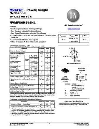
MOSFET - Power, Single N-Channel 80 V, 8.8 mW, 59 A NVMFS6H848NL Features www.onsemi.com Small Footprint (5x6 mm) for Compact Design Low RDS(on) to Minimize Conduction Losses Low QG and Capacitance to Minimize Driver Losses NVMFS6H848NLWF - Wettable Flank Option for Enhanced Optical V(BR)DSS RDS(ON) MAX ID MAX Inspection 8.8 mW @ 10 V AEC-Q101 Qualified and PPAP... See More ⇒
8.17. Size:178K onsemi
nvmfs6h852nl.pdf
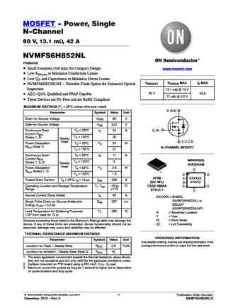
MOSFET - Power, Single N-Channel 80 V, 13.1 mW, 42 A NVMFS6H852NL Features Small Footprint (5x6 mm) for Compact Design www.onsemi.com Low RDS(on) to Minimize Conduction Losses Low QG and Capacitance to Minimize Driver Losses V(BR)DSS RDS(ON) MAX ID MAX NVMFS6H852NLWF - Wettable Flank Option for Enhanced Optical Inspection 13.1 mW @ 10 V 80 V 42 A AEC-Q101 Quali... See More ⇒
8.18. Size:178K onsemi
nvmfs6h858n.pdf

MOSFET - Power, Single N-Channel 80 V, 20.7 mW, 32 A NVMFS6H858N Features www.onsemi.com Small Footprint (5x6 mm) for Compact Design Low RDS(on) to Minimize Conduction Losses Low QG and Capacitance to Minimize Driver Losses NVMFS6H858NWF - Wettable Flank Option for Enhanced Optical V(BR)DSS RDS(ON) MAX ID MAX Inspection 80 V 20.7 mW @ 10 V 32 A AEC-Q101 Qualifie... See More ⇒
Detailed specifications: NVMFS5C673NL
, NVMFS5C677NL
, NVMFS5C680NL
, NVMFS5C682NL
, NVMFS5H600NL
, NVMFS5H663NL
, NVMFS5H663NLWF
, NVMFS6B14NL
, AO4407
, NVMFS6D1N08H
, NVMFS6H800NL
, NVMFS6H801N
, NVMFS6H801NL
, NVMFS6H818N
, NVMFS6H818NL
, NVMFS6H824N
, NVMFS6H824NL
.
Keywords - NVMFS6B75NL MOSFET specs
NVMFS6B75NL cross reference
NVMFS6B75NL equivalent finder
NVMFS6B75NL pdf lookup
NVMFS6B75NL substitution
NVMFS6B75NL replacement
Need a MOSFET replacement?
Our guide shows you how to find a perfect substitute by comparing key parameters and specs
