PJM3400NSC Specs and Replacement
Type Designator: PJM3400NSC
Type of Transistor: MOSFET
Type of Control Channel: N-Channel
Absolute Maximum Ratings
Pd ⓘ - Maximum Power Dissipation: 1.4 W
|Vds|ⓘ - Maximum Drain-Source Voltage: 30 V
|Vgs|ⓘ - Maximum Gate-Source Voltage: 12 V
|Id| ⓘ - Maximum Drain Current: 5.8 A
Tj ⓘ - Maximum Junction Temperature: 150 °C
Electrical Characteristics
tr ⓘ - Rise Time: 4.8 nS
Cossⓘ - Output Capacitance: 100 pF
RDSonⓘ - Maximum Drain-Source On-State Resistance: 0.027 Ohm
Package: SOT23
PJM3400NSC substitution
- MOSFET ⓘ Cross-Reference Search
PJM3400NSC datasheet
pjm3400nsc.pdf
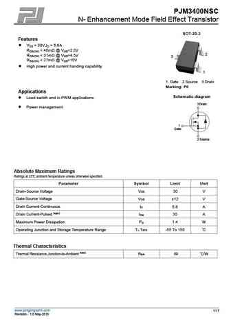
PJM3400NSC N- Enhancement Mode Field Effect Transistor SOT-23-3 Features VDS = 30V,ID = 5.8A RDS(ON) ... See More ⇒
pjm3400nsa.pdf
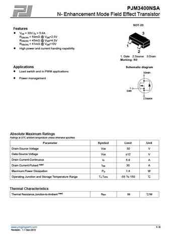
PJM3400NSA N- Enhancement Mode Field Effect Transistor SOT-23 Features VDS = 30V,ID = 5.8A RDS(ON) ... See More ⇒
pjm3401psc.pdf
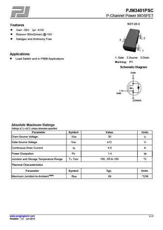
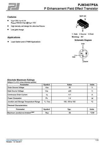
PJM3401PSC P-Channel Power MOSFET SOT-23-3 Features VDS= -30V I = -4.5A D RDS(ON)= 60m (max) @-10V 2 Halogen and Antimony Free 3 1 Applications 1. Gate 2.Source 3.Drain Load Switch and in PWM Applications Marking P1 Schematic Diagram Drain 3 1 Gate Source 2 Absolute Maximum Ratings Ratings at TA =25 unless otherwise specified. Parameter Symbol Valu... See More ⇒
pjm3401psa.pdf
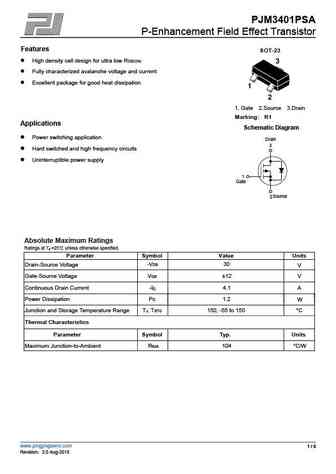
PJM3401PSA P-Enhancement Field Effect Transistor Features SOT-23 High density cell design for ultra low RDS(ON) Fully characterized avalanche voltage and current Excellent package for good heat dissipation 1. Gate 2.Source 3.Drain Marking R1 Applications Schematic Diagram Power switching application Drain 3 Hard switched and high frequency circuits Unint... See More ⇒
Detailed specifications: PJM2301PSA-S, PJM2302NSA, PJM2302NSA-S, PJM2305PSA, PJM2309PSA, PJM2309PSC, PJM2319PSA, PJM3400NSA, IRF4905, PJM3401PSA, PJM3401PSC, PJM3407PSA, PJM3415PSA, PJM84PSA, EM6M2, LSK3019FP8, LSK3541FS8
Keywords - PJM3400NSC MOSFET specs
PJM3400NSC cross reference
PJM3400NSC equivalent finder
PJM3400NSC pdf lookup
PJM3400NSC substitution
PJM3400NSC replacement
Can't find your MOSFET? Learn how to find a substitute transistor by analyzing voltage, current and package compatibility
History: SMK0965FJ | PJM2309PSC
🌐 : EN ES РУ

LIST
Last Update
MOSFET: ASU70R600E | ASU65R850E | ASU65R550E | ASU65R350E | ASR65R120EFD | ASR65R046EFD | ASQ65R046EFD | ASM65R280E | ASM60R330E | ASE70R950E
Popular searches
bc547 datasheet | k3797 mosfet | bs170 datasheet | tip41c | irfp460 | irfz44n mosfet | lm317t datasheet | irf540