2301P Specs and Replacement
Type Designator: 2301P
Type of Transistor: MOSFET
Type of Control Channel: P-Channel
Absolute Maximum Ratings
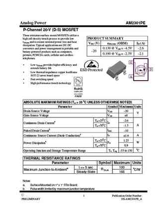
Pd ⓘ - Maximum Power Dissipation: 0.84 W
|Vds|ⓘ - Maximum Drain-Source Voltage: 20 V
|Vgs|ⓘ - Maximum Gate-Source Voltage: 12 V
|Id| ⓘ - Maximum Drain Current: 2.8 A
Tj ⓘ - Maximum Junction Temperature: 150 °C
Electrical Characteristics
tr ⓘ - Rise Time: 6.1 nS
Cossⓘ - Output Capacitance: 68 pF
RDSonⓘ - Maximum Drain-Source On-State Resistance: 0.135 Ohm
Package: SOT23
2301P substitution
- MOSFET ⓘ Cross-Reference Search
2301P datasheet
2301p.pdf
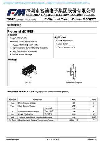
FM , FM WWW.SZLCSC.COM, SHEN ZHEN FINE MADE ELECTRONICS GROUP CO., LTD. 2301P( S&CIC1974) P-Channel Trench Power MOSFET Description P-channel MOSFET Features Application V =-20V, I =-2.8A D... See More ⇒
nx2301p.pdf
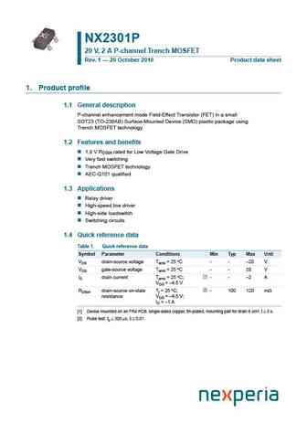
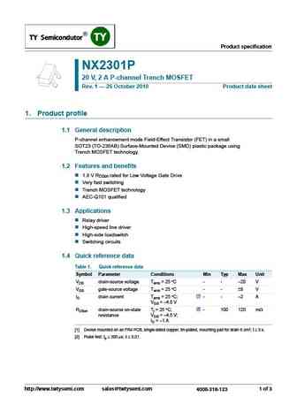
NX2301P 20 V, 2 A P-channel Trench MOSFET Rev. 1 26 October 2010 Product data sheet 1. Product profile 1.1 General description P-channel enhancement mode Field-Effect Transistor (FET) in a small SOT23 (TO-236AB) Surface-Mounted Device (SMD) plastic package using Trench MOSFET technology. 1.2 Features and benefits 1.8 V RDSon rated for Low Voltage Gate Drive Very fast switching... See More ⇒
smg2301p.pdf
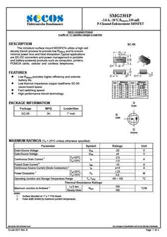
SMG2301P -2.6 A, -20 V, RDS(ON) 130 m P-Channel Enhancement MOSFET Elektronische Bauelemente RoHS Compliant Product A suffix of -C specifies halogen & lead-free DESCRIPTION SC-59 The miniature surface mount MOSFETs utilize a high cell density trench process to provide low RDS(on) and to ensure A L minimal power loss and heat dissipation.Typical applications 3 3... See More ⇒
am2301p.pdf
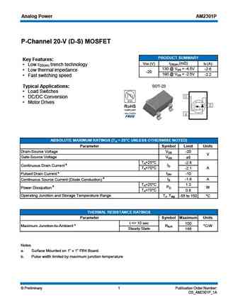
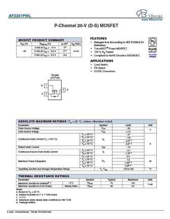
Analog Power AM2301P P-Channel 20-V (D-S) MOSFET PRODUCT SUMMARY Key Features rDS(on) (m ) VDS (V) ID (A) Low r trench technology DS(on) 130 @ VGS = -4.5V -2.6 Low thermal impedance -20 190 @ VGS = -2.5V -2.2 Fast switching speed SOT-23 Typical Applications Load Switches DC/DC Conversion Motor Drives ABSOLUTE MAXIMUM RATINGS (TA = 25 C UNLE... See More ⇒
Detailed specifications: D2N65, D4N65, F10N65, F12N65, .8205A, .8205S, .8205P, 2060K., IRF2807, 2302P, 3050K, 3060K, 3080K, 3090K, 3415E, 4080K, 6888K
Keywords - 2301P MOSFET specs
2301P cross reference
2301P equivalent finder
2301P pdf lookup
2301P substitution
2301P replacement
Step-by-step guide to finding a MOSFET replacement. Cross-reference parts and ensure compatibility for your repair or project.
History: AOTF2144L | 3N70L-TF3-T | STT8205S
🌐 : EN ES РУ

LIST
Last Update
MOSFET: AUB034N10 | AUB033N08BG | AUB026N085 | AUA062N08BG | AUA060N08AG | AUA056N08BGL | AUA039N10 | ASW80R290E | ASW65R120EFD | ASW65R110E
Popular searches
2sc2078 transistor | bc558 datasheet | p75nf75 mosfet | ao4407a | mpsa06 datasheet | bc548 pinout | bdw94c | bd140 transistor