SE30P12 Specs and Replacement
Type Designator: SE30P12
Type of Transistor: MOSFET
Type of Control Channel: P-Channel
Absolute Maximum Ratings
Pd ⓘ - Maximum Power Dissipation: 2 W
|Vds|ⓘ - Maximum Drain-Source Voltage: 30 V
|Vgs|ⓘ - Maximum Gate-Source Voltage: 20 V
|Id| ⓘ - Maximum Drain Current: 11 A
Tj ⓘ - Maximum Junction Temperature: 150 °C
Electrical Characteristics
tr ⓘ - Rise Time: 16.5 nS
Cossⓘ - Output Capacitance: 945 pF
RDSonⓘ - Maximum Drain-Source On-State Resistance: 0.015 Ohm
Package: SOP8
SE30P12 substitution
- MOSFET ⓘ Cross-Reference Search
SE30P12 datasheet
se30p12.pdf
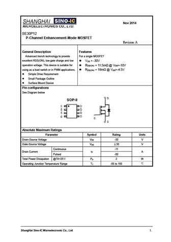
Nov 2014 SE30P12 P-Channel Enhancement-Mode MOSFET Revision A General Description Features Advanced trench technology to provide For a single MOSFET excellent RDS(ON), low gate charge and low V = -30V DS operation voltage. This device is suitable for R =11.5m @V =-10V DS(ON) GS using as a load switch or in PWM applications. R =18m @V =-4.5V DS(ON) GS Simple... See More ⇒
se30p12d.pdf
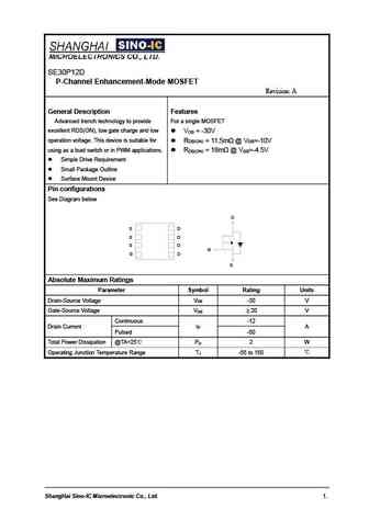
SE30P12D P-Channel Enhancement-Mode MOSFET Revision A General Description Features Advanced trench technology to provide For a single MOSFET excellent RDS(ON), low gate charge and low V = -30V DS operation voltage. This device is suitable for R =11.5m @V =-10V DS(ON) GS using as a load switch or in PWM applications. R =18m @V =-4.5V DS(ON) GS Simple Drive Re... See More ⇒
se30p50.pdf
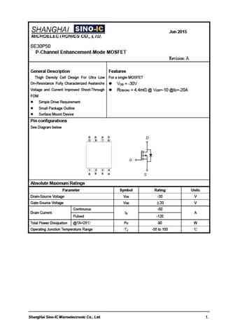
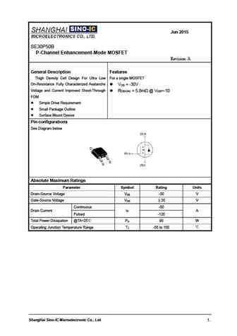
Jun 2015 SE30P50 P-Channel Enhancement-Mode MOSFET Revision A General Description Features Thigh Density Cell Design For Ultra Low For a single MOSFET On-Resistance Fully Characterized Avalanche V = -30V DS Voltage and Current Improved Shoot-Through R =4.4m @V =-10 @I =-20A DS(ON) GS D FOM Simple Drive Requirement Small Package Outline Surface Mount Device... See More ⇒
se30p09d.pdf
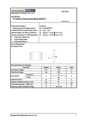
Nov 2014 SE30P09D P-Channel Enhancement-Mode MOSFET Revision A General Description Features Advanced trench technology to provide For a single MOSFET excellent RDS(ON), low gate charge and low V = -30V DS operation voltage. This device is suitable for R = 15m @ V =-10V DS(ON) GS using as a load switch or in PWM applications. R = 21m @ V =-4.5V DS(ON) GS Simpl... See More ⇒
Detailed specifications: SE472, SE3060D, SE3080A, SE3080K, SE3080G, SE3082G, SE3090K, SE30P09D, IRFP064N, SE30P12D, SE30P50, SE30P50B, SE3205A, SE3401B, SE3N150P, SE40120A, SE40150
Keywords - SE30P12 MOSFET specs
SE30P12 cross reference
SE30P12 equivalent finder
SE30P12 pdf lookup
SE30P12 substitution
SE30P12 replacement
Need a MOSFET replacement? Our guide shows you how to find a perfect substitute by comparing key parameters and specs
History: NTMFS4841N | ELM544599A | AP70WN2K8I | TK32A12N1 | SSA50R060S | LPSA3487
🌐 : EN ES РУ

LIST
Last Update
MOSFET: AUB062N08BG | AUB060N08AG | AUB056N10 | AUB056N08BGL | AUB050N085 | AUB050N055 | AUB045N12 | AUB045N10BT | AUB039N10 | AUB034N10
Popular searches
2n3403 | 2sa750 | tip117 | 2n3643 | 2sc2078 transistor equivalent | 2sc2073 | a608 transistor | c536 transistor