20P06-TO252 Specs and Replacement
Type Designator: 20P06-TO252
Type of Transistor: MOSFET
Type of Control Channel: P-Channel
Absolute Maximum Ratings
Pd ⓘ - Maximum Power Dissipation: 34 W
|Vds|ⓘ - Maximum Drain-Source Voltage: 60 V
|Vgs|ⓘ - Maximum Gate-Source Voltage: 20 V
|Id| ⓘ - Maximum Drain Current: 30 A
Tj ⓘ - Maximum Junction Temperature: 175 °C
Electrical Characteristics
tr ⓘ - Rise Time: 15 nS
Cossⓘ - Output Capacitance: 120 pF
RDSonⓘ - Maximum Drain-Source On-State Resistance: 0.061 typ Ohm
Package: TO252
20P06-TO252 substitution
- MOSFET ⓘ Cross-Reference Search
20P06-TO252 datasheet
20p06-to252.pdf

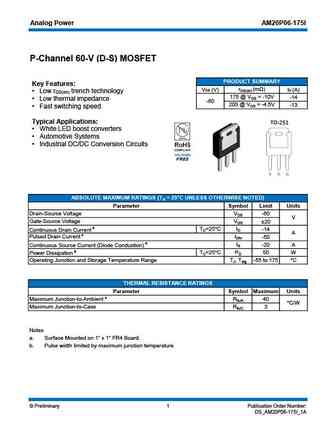
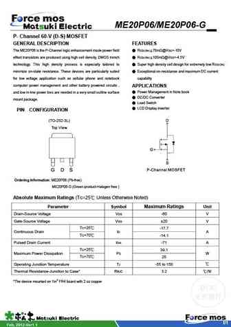
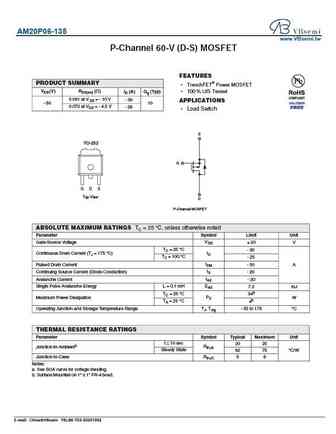
20P06 TO252 www.VBsemi.tw P-Channel 60-V (D-S) MOSFET FEATURES PRODUCT SUMMARY TrenchFET Power MOSFET VDS (V) RDS(on) ( ) ID (A) Qg (Typ) 100 % UIS Tested 0.061 at VGS = - 10 V - 30 APPLICATIONS - 60 10 0.072 at VGS = - 4.5 V - 26 Load Switch S TO-252 G G D S Top View D P-Channel MOSFET ABSOLUTE MAXIMUM RATINGS TC = 25 C, unless otherwise noted Parameter S... See More ⇒
sqm120p06-07l.pdf
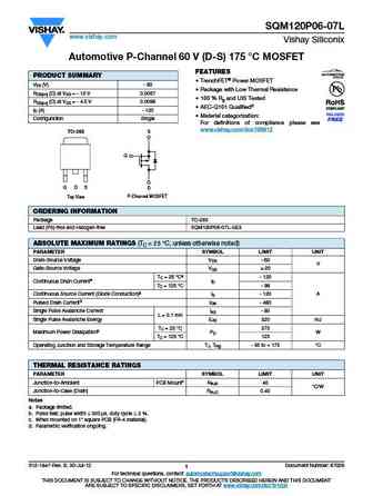
SQM120P06-07L www.vishay.com Vishay Siliconix Automotive P-Channel 60 V (D-S) 175 C MOSFET FEATURES PRODUCT SUMMARY TrenchFET Power MOSFET VDS (V) - 60 Package with Low Thermal Resistance RDS(on) ( ) at VGS = - 10 V 0.0067 100 % Rg and UIS Tested RDS(on) ( ) at VGS = - 4.5 V 0.0088 AEC-Q101 Qualifiedd ID (A) - 120 Material categorization Configurat... See More ⇒
ssd20p06-135d.pdf
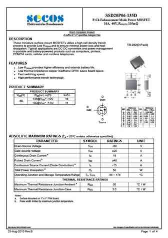
SSD20P06-135D P-Ch Enhancement Mode Power MOSFET 16A, -60V, RDS(ON) 135m Elektronische Bauelemente RoHS Compliant Product A suffix of -C specifies halogen free DESCRIPTION These miniature surface mount MOSFETs utilize a high cell density trench TO-252(D-Pack) process to provide Low RDS(on) and to ensure minimal power loss and heat dissipation. Typical applications are... See More ⇒
am20p06-135d.pdf
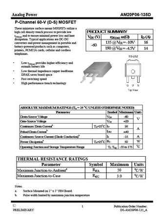
Analog Power AM20P06-135D P-Channel 60-V (D-S) MOSFET These miniature surface mount MOSFETs utilize a high cell density trench process to provide low PRODUCT SUMMARY rDS(on) and to ensure minimal power loss and heat VDS (V) rDS(on) m( )ID (A) dissipation. Typical applications are DC-DC 135 @ VGS = -10V 16 converters and power management in portable and -60 battery-powered produc... See More ⇒
Detailed specifications: 2SK4081D, 13N10, 15N10-TO251, 1812, 1N60L-TM3-T, 20N03L-TO252, 20N06L-TO252, 20N3LG-TO251, AO3401, 25N06L-TN3, 25NF20, 2N0623, 2N65-TO252, 2SJ530STL, 2SJ598-Z-E1, 2SK1589-T1B, 2SK1623
Keywords - 20P06-TO252 MOSFET specs
20P06-TO252 cross reference
20P06-TO252 equivalent finder
20P06-TO252 pdf lookup
20P06-TO252 substitution
20P06-TO252 replacement
Learn how to find the right MOSFET substitute. A guide to cross-reference, check specs and replace MOSFETs in your circuits.
History: SVD3205T | APM2701AC | CMI100N04 | CS7N65FA9R | VS1606GS | SM1691OSCS
🌐 : EN ES РУ

LIST
Last Update
MOSFET: AUB034N10 | AUB033N08BG | AUB026N085 | AUA062N08BG | AUA060N08AG | AUA056N08BGL | AUA039N10 | ASW80R290E | ASW65R120EFD | ASW65R110E
Popular searches
2sa1011 | 2sa1283 | 2sb646 | 2sc1885 datasheet | 2sc2580 | 2sc710 | 2sc968 | 2sd217