APM2054NDC Specs and Replacement
Type Designator: APM2054NDC
Type of Transistor: MOSFET
Type of Control Channel: N-Channel
Absolute Maximum Ratings
Pd ⓘ - Maximum Power Dissipation: 2.5 W
|Vds|ⓘ - Maximum Drain-Source Voltage: 30 V
|Vgs|ⓘ - Maximum Gate-Source Voltage: 20 V
|Id| ⓘ - Maximum Drain Current: 6.8 A
Tj ⓘ - Maximum Junction Temperature: 150 °C
Electrical Characteristics
tr ⓘ - Rise Time: 10 nS
Cossⓘ - Output Capacitance: 220 pF
RDSonⓘ - Maximum Drain-Source On-State Resistance: 0.033 Ohm
Package: SOT89
APM2054NDC substitution
- MOSFET ⓘ Cross-Reference Search
APM2054NDC datasheet
apm2054ndc.pdf
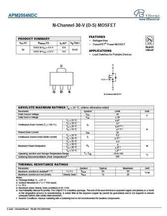
APM2054NDC www.VBsemi.tw N-Channel 30-V (D-S) MOSFET FEATURES PRODUCT SUMMARY Halogen-free VDS (V) RDS(on) ( ) ID (A)a Qg (Typ.) TrenchFET Power MOSFET 0.022 at VGS = 4.5 V 6.8 RoHS 30 10 nC COMPLIANT APPLICATIONS 0.027 at VGS = 2.5 V 6.0 Load Switches for Portable Devices D D G S G D S N-Channel MOSFET ABSOLUTE MAXIMUM RATINGS TA = 25 C, unless otherwis... See More ⇒
apm2054n.pdf
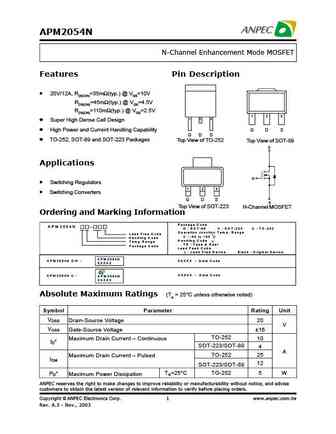
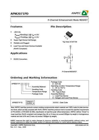
APM2054N N-Channel Enhancement Mode MOSFET Features Pin Description 20V/12A, RDS(ON)=35m (typ.) @ VGS=10V RDS(ON)=45m (typ.) @ VGS=4.5V RDS(ON)=110m (typ.) @ VGS=2.5V 1 2 3 1 2 3 Super High Dense Cell Design High Power and Current Handling Capability G D S G D S TO-252, SOT-89 and SOT-223 Packages To... See More ⇒
apm2055nu.pdf
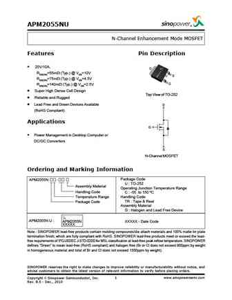
APM2055NU N-Channel Enhancement Mode MOSFET Features Pin Description 20V/10A, D RDS(ON)=55m (Typ.) @ VGS=10V S RDS(ON)=75m (Typ.) @ VGS=4.5V G RDS(ON)=140m (Typ.) @ VGS=2.5V Super High Dense Cell Design Top View of TO-252 Reliable and Rugged Lead Free and Green Devices Available D (RoHS Compliant) Applications G Power Management in Desktop Computer o... See More ⇒
apm2014n.pdf
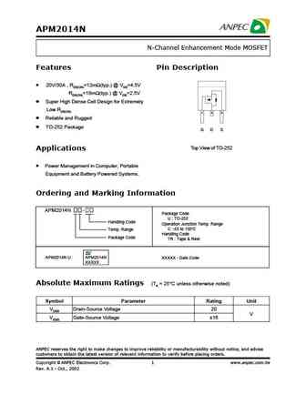
APM2014N N-Channel Enhancement Mode MOSFET Features Pin Description 20V/30A , RDS(ON)=12m (typ.) @ VGS=4.5V RDS(ON)=18m (typ.) @ VGS=2.5V Super High Dense Cell Design for Extremely Low RDS(ON) 1 2 3 Reliable and Rugged TO-252 Package G D S Top View of TO-252 Applications Power Management in Comput... See More ⇒

Detailed specifications: AP85U03GH, AP9435GG, AP9435GK, AP9435K, AP9563M, AP9579GM, AP9997GH, APM1110NUC, AO4407A, APM2300CAC, APM2301AC, APM2303AC, APM2305AC, APM2308AC, APM2309AC, APM2314AC, APM2315AC
Keywords - APM2054NDC MOSFET specs
APM2054NDC cross reference
APM2054NDC equivalent finder
APM2054NDC pdf lookup
APM2054NDC substitution
APM2054NDC replacement
Step-by-step guide to finding a MOSFET replacement. Cross-reference parts and ensure compatibility for your repair or project.
History: VB8338
🌐 : EN ES РУ

LIST
Last Update
MOSFET: AUB062N08BG | AUB060N08AG | AUB056N10 | AUB056N08BGL | AUB050N085 | AUB050N055 | AUB045N12 | AUB045N10BT | AUB039N10 | AUB034N10
Popular searches
2n2222a transistor equivalent | 2sc2509 | 2n1815 | 2sa1103 | 2sb435 | 2sc1096 | 2sc2058 | a1693 datasheet