APM4050PUC Specs and Replacement
Type Designator: APM4050PUC
Type of Transistor: MOSFET
Type of Control Channel: P-Channel
Absolute Maximum Ratings
Pd ⓘ - Maximum Power Dissipation: 136 W
|Vds|ⓘ - Maximum Drain-Source Voltage: 40 V
|Vgs|ⓘ - Maximum Gate-Source Voltage: 20 V
|Id| ⓘ - Maximum Drain Current: 50 A
Tj ⓘ - Maximum Junction Temperature: 175 °C
Electrical Characteristics
tr ⓘ - Rise Time: 12 nS
Cossⓘ - Output Capacitance: 508 pF
Rds ⓘ - Maximum Drain-Source On-State Resistance: 0.014 Ohm
Package: TO252
APM4050PUC substitution
- MOSFET ⓘ Cross-Reference Search
APM4050PUC datasheet
apm4050puc.pdf
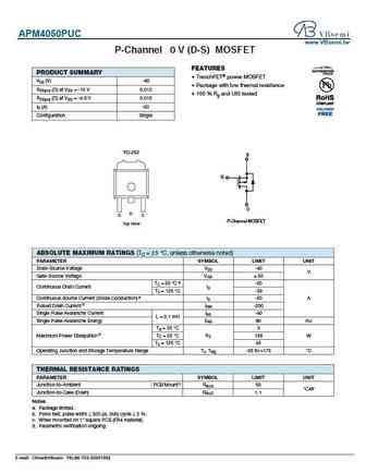
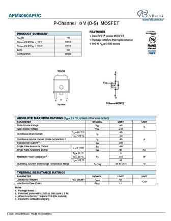
APM4050PUC www.VBsemi.tw P-Channel 4 0 V (D-S) MOSFET FEATURES PRODUCT SUMMARY TrenchFET power MOSFET VDS (V) -40 Package with low thermal resistance RDS(on) ( ) at VGS = -10 V 0.012 100 % Rg and UIS tested RDS(on) ( ) at VGS = -4.5 V 0.015 ID (A) -50 Configuration Single TO-252 S G D D G S P-Channel MOSFET Top View ABSOLUTE MAXIMUM RATINGS (TC = 25 C, u... See More ⇒
apm4050pu.pdf
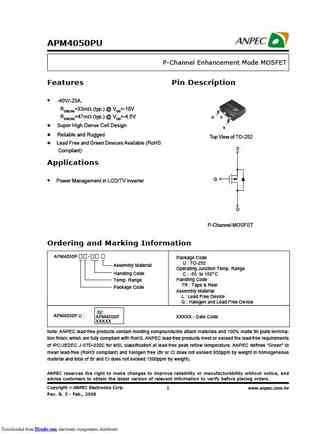
APM4050PU P-Channel Enhancement Mode MOSFET Features Pin Description -40V/-25A, RDS(ON)=33m (typ.) @ VGS=-10V G D RDS(ON)=47m (typ.) @ VGS=-4.5V Super High Dense Cell Design S Reliable and Rugged Top View of TO-252 Lead Free and Green Devices Available (RoHS S Compliant) Applications G Power Management in LCD/TV Inverter D P-Channel MOSFET Ordering and Mar... See More ⇒
apm4050apu.pdf
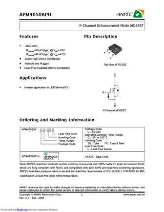
APM4050APU P-Channel Enhancement Mode MOSFET Features Pin Description -40V/-25A, RDS(ON)=33m (typ.) @ VGS=-10V G D RDS(ON)=47m (typ.) @ VGS=-4.5V S Super High Dense Cell Design Reliable and Rugged Top View of TO-252 Lead Free Available (RoHS Compliant) S Applications Inverter application in LCD Monitor/TV G D P-Channel MOSFET Ordering and Marking Informatio... See More ⇒
apm4050bpu.pdf
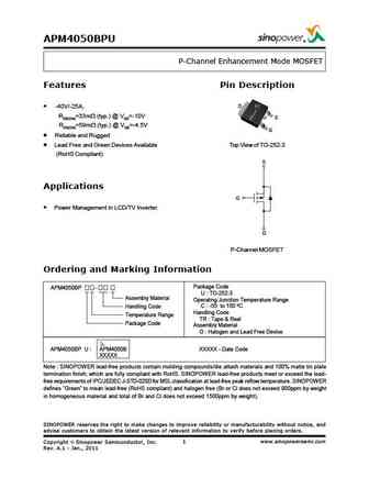
APM4050BPU P-Channel Enhancement Mode MOSFET Features Pin Description D -40V/-25A, RDS(ON)=33m (typ.) @ VGS=-10V S RDS(ON)=59m (typ.) @ VGS=-4.5V G Reliable and Rugged Lead Free and Green Devices Available Top View of TO-252-3 (RoHS Compliant) S Applications G Power Management in LCD/TV Inverter. D P-Channel MOSFET Ordering and Marking Information Package... See More ⇒
Detailed specifications: APM2323AAC , APM2701ACC-TRG , APM3009NUC , APM3040NDC , APM3054NUC , APM3055LUC , APM4010NUC , APM4050APUC , IRFP260N , APM4303KC , APM4330KC , APM4532KC , APM4550KC , APM4828KC-TRL , APM4927KC , APM4953KC , APM7313KC .
History: 2SK1904
Keywords - APM4050PUC MOSFET specs
APM4050PUC cross reference
APM4050PUC equivalent finder
APM4050PUC pdf lookup
APM4050PUC substitution
APM4050PUC replacement
Step-by-step guide to finding a MOSFET replacement. Cross-reference parts and ensure compatibility for your repair or project.
History: 2SK1904
🌐 : EN ES РУ

LIST
Last Update
MOSFET: HAF1008S | HAF1008L | EMZB08P03H | CS30N20FA9R | AOT66613L | AOSP21313C | AOSP21311C | AOB66918L | AO3415C | AOTF20N40L
Popular searches
sm4377 mosfet datasheet | tip31c reemplazo | 2sa906 | c2389 transistor | c2634 transistor | mdp1991 datasheet | 40636 transistor | ao3407 datasheet