ISL9N308AD3ST Specs and Replacement
Type Designator: ISL9N308AD3ST
Type of Transistor: MOSFET
Type of Control Channel: N-Channel
Absolute Maximum Ratings
Pd ⓘ - Maximum Power Dissipation: 205 W
|Vds|ⓘ - Maximum Drain-Source Voltage: 30 V
|Vgs|ⓘ - Maximum Gate-Source Voltage: 20 V
|Id| ⓘ - Maximum Drain Current: 80 A
Tj ⓘ - Maximum Junction Temperature: 175 °C
Electrical Characteristics
tr ⓘ - Rise Time: 11 nS
Cossⓘ - Output Capacitance: 525 pF
RDSonⓘ - Maximum Drain-Source On-State Resistance: 0.005 typ Ohm
Package: TO252
ISL9N308AD3ST substitution
- MOSFET ⓘ Cross-Reference Search
ISL9N308AD3ST datasheet
isl9n308ad3st.pdf
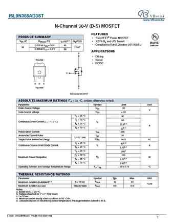
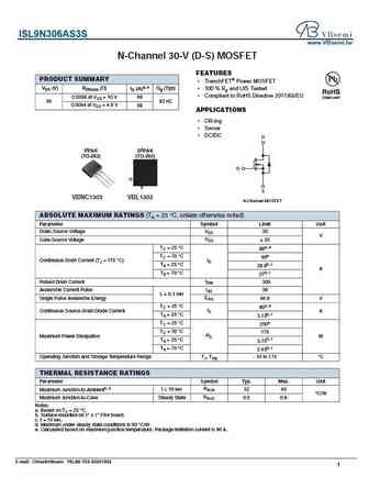
ISL9N308AD3ST www.VBsemi.tw N-Channel 30-V (D-S) MOSFET FEATURES PRODUCT SUMMARY TrenchFET Power MOSFET VDS (V) RDS(on) ( ) ID (A)a, e Qg (Typ) 100 % Rg and UIS Tested Compliant to RoHS Directive 2011/65/EU 0.005 at VGS = 10 V 80 30 31 nC 0.006 at VGS = 4.5 V 68 APPLICATIONS D OR-ing TO-252 Server DC/DC G G D S Top View S N-Channel MOSFET A... See More ⇒
isl9n308ad3.pdf
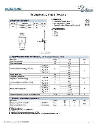
ISL9N308AD3 www.VBsemi.tw N-Channel 30-V (D-S) MOSFET FEATURES PRODUCT SUMMARY TrenchFET Power MOSFET VDS (V) RDS(on) ( ) ID (A)a, e Qg (Typ) 100 % Rg and UIS Tested Compliant to RoHS Directive 2011/65/EU 0.005 at VGS = 10 V 80 30 31 nC 0.006 at VGS = 4.5 V 68 APPLICATIONS D OR-ing TO-252 Server DC/DC G G D S Top View S N-Channel MOSFET ABS... See More ⇒
isl9n302as3st.pdf
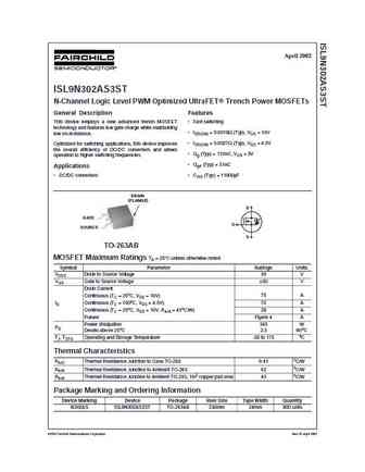
April 2002 ISL9N302AS3ST N-Channel Logic Level PWM Optimized UltraFET Trench Power MOSFETs General Description Features This device employs a new advanced trench MOSFET Fast switching technology and features low gate charge while maintaining rDS(ON) =0.0019 (Typ), VGS =10V low on-resistance. rDS(ON) =0.0027 (Typ), VGS =4.5V Optimized for switching applications, this... See More ⇒
isl9n303ap3.pdf

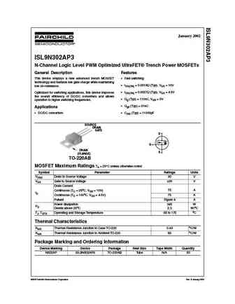
September 2002 PWM Optimized ISL9N303AP3 / ISL9N303AS3ST / ISL9N303AS3 N-Channel Logic Level UltraFET Trench MOSFETs 30V, 75A, 3.2m General Description Features This device employs a new advanced trench MOSFET Fast switching technology and features low gate charge while maintaining rDS(ON) = 0.0026 (Typ), VGS = 10V low on-resistance. rDS(ON) = 0.004 (Typ), VGS =... See More ⇒

Detailed specifications: MCH3409-TL, KD2306A, KD2310, KD3400SRG, IRLU110P, IRLU3103P, IRLU3410P, ISL9N306AD3S, 7N65, ISL9N308AD3, K1307, K2543, K2543-FP, K3569, K3569-FP, K4145, KD2301
Keywords - ISL9N308AD3ST MOSFET specs
ISL9N308AD3ST cross reference
ISL9N308AD3ST equivalent finder
ISL9N308AD3ST pdf lookup
ISL9N308AD3ST substitution
ISL9N308AD3ST replacement
Need a MOSFET replacement? Our guide shows you how to find a perfect substitute by comparing key parameters and specs
🌐 : EN ES РУ

LIST
Last Update
MOSFET: AUB062N08BG | AUB060N08AG | AUB056N10 | AUB056N08BGL | AUB050N085 | AUB050N055 | AUB045N12 | AUB045N10BT | AUB039N10 | AUB034N10
Popular searches
2n3392 | 2n2369a | 2sc733 | a933 transistor | d209l | irfb4321 | 2n333 | c3852